Surface emitting laser element, surface emitting laser array, optical scanning apparatus, image forming apparatus, and optical communication system

Active Publication Date: 2008-03-06
RICOH KK
View PDF20 Cites 51 Cited by
  • Summary
  • Abstract
  • Description
  • Claims
  • Application Information

AI Technical Summary

Benefits of technology

[0009] One aspect of the present invention is related to providing a

Problems solved by technology

However, since the volume of the active layer of the VCSEL is relatively small, the optical

Method used


Image

  • Surface emitting laser element, surface emitting laser array, optical scanning apparatus, image forming apparatus, and optical communication system
  • Surface emitting laser element, surface emitting laser array, optical scanning apparatus, image forming apparatus, and optical communication system
  • Surface emitting laser element, surface emitting laser array, optical scanning apparatus, image forming apparatus, and optical communication system

Examples


Example

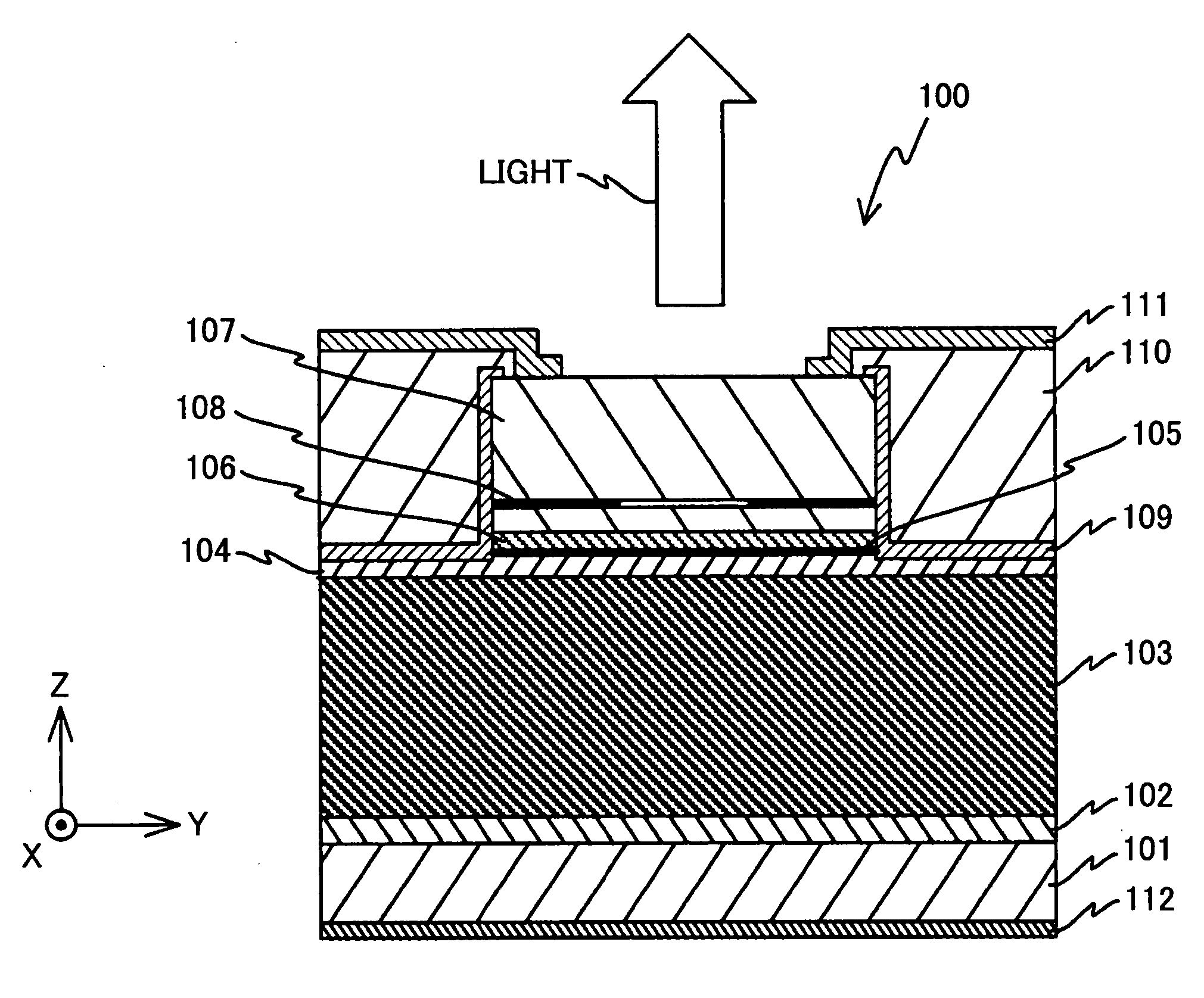
[0044] A first embodiment of the present invention is described below with reference to FIGS. 1-5. FIG. 1 is a diagram illustrating an overall configuration of a vertical cavity surface emitting laser element 100 according to the first embodiment. It is noted that in the following descriptions, a laser oscillating direction is referred to as Z axis direction, and two orthogonal directions that form a plane that is perpendicular to the Z axis direction are referred to as X axis direction and Y axis direction.

[0045] The illustrated surface emitting laser element 100 is a 780-nm-band surface emitting laser element that has a substrate 101 and semiconductor layers including a buffer layer 102, a semiconductor multilayer reflector (referred to as ‘lower DBR’ hereinafter) 103, a lower spacer layer 104, a multi-quantum well active layer 105, an upper spacer layer 106, and an upper DBR 107, for example, that are successively layered on the substrate 101 in this order. It is noted that in t...

Example

Second Embodiment

[0095] A second embodiment of the present invention is described below with reference to FIGS. 11 and 12. FIG. 11 is a diagram showing an overall configuration of a vertical cavity surface emitting laser element 200 according to the second embodiment of the present invention.

[0096] The illustrated surface emitting laser element 200 according to the second embodiment is a 1.3-μm-band surface emitting laser element that has a substrate 201 and semiconductor layers including a buffer layer 202, a first lower DBR 203a, a second lower DBR 203b, a lower spacer layer 204, a multi-quantum well active layer 205, an upper spacer layer 206, and an upper DBR 207, for example, that are successively layered on the substrate 201 in this order. It is noted that in the following descriptions, the above multilayer structure of the semiconductor layers are referred to as ‘second multilayer structure’ hereinafter.

[0097] In the present example, the substrate 201 is made of n-GaAs.

[0...

Example

[0121] A third embodiment of the present invention is described below with reference to FIGS. 13 and 14. FIG. 13 is a diagram showing a configuration of a vertical cavity surface emitting laser element 300 according to the third embodiment of the present invention.

[0122] The illustrated surface emitting laser element 300 is a 1.3-μm-band junction-down type surface emitting laser element that has a substrate 301 and semiconductor layers including a buffer layer 302, a lower DBR 303, a lower spacer layer 304, a DQW quantum well active layer 305, an upper spacer layer 306, and an upper DBR 307, for example, that are successively layered on the substrate 301 in this order. It is noted that in the following descriptions, the above multilayer structure of the semiconductor layers is referred to as ‘third multilayer structure’ hereinafter.

[0123] In a junction-down type surface emitting laser element, a heat sink is connected to the substrate surface side at which a light emitting layer i...


PUM


Abstract

A vertical cavity surface emitting laser element is disclosed that includes a substrate, a first semiconductor multilayer reflector including plural pairs of layers having differing refractive indexes and thermal resistances, a resonator region including an active layer, and a second semiconductor multilayer reflector including plural pairs of layers having differing refractive indexes and thermal resistances. At least one pair of layers of the first semiconductor multilayer reflector and/or the second semiconductor multilayer reflector includes a first layer with a lower thermal resistance that has an optical thickness greater than ¼ of the oscillation wavelength and a second layer with a higher thermal resistance that has an optical thickness less than ¼ of the oscillation wavelength. The sum of the optical thickness of the first layer and the optical thickness of the second layer is equal to m/4 times the oscillation wavelength (m: even number≧2).

Description

BACKGROUND OF THE INVENTION [0001] 1. Field of the Invention [0002] The present invention relates to a surface emitting laser element that emits light in a vertical direction with respect to a substrate, a surface emitting laser array including such surface emitting laser elements, and an optical scanning apparatus, an image forming apparatus, and an optical communication system that use light emitted from such surface emitting laser element or surface emitting laser array. [0003] 2. Description of the Related Art [0004] A vertical cavity surface emitting laser (VCSEL) is a semiconductor laser that emits light in a vertical direction with respect to a substrate. Since the VCSEL does not require a cleavage process, may be integrated into a two-dimensional parallel arrangement, and may be easily inspected, it is suitably used in various consumer appliances such as the light source of an image forming apparatus, the light source of an optical pickup device, the optical communication li...

Claims


Application Information

Patent Timeline
IPC IPC(8): H01S5/18B41J27/00
CPCB41J2/45B41J2/473G02B6/4249H01S5/0207H01S5/02461H01S5/423H01S5/18308H01S5/18311H01S5/1833H01S5/18358H01S5/18305
Inventor MOTOMURA, HIROSHIJIKUTANI, NAOTOSATO, SHUNICHI
Owner RICOH KK
Why Eureka
Try Eureka