Stacked semiconductor device

a semiconductor device and stacked technology, applied in semiconductor devices, semiconductor/solid-state device details, electrical devices, etc., can solve the problems of physical limitation of memory cell miniaturization, affecting the operation speed of memory cells, reducing yield, etc., to achieve the effect of suppressing a power source voltage drop, reducing voltage drop level, and easy supply of power source potential

Active Publication Date: 2007-08-09
MICRON TECH INC
View PDF27 Cites 86 Cited by
  • Summary
  • Abstract
  • Description
  • Claims
  • Application Information

AI Technical Summary

Benefits of technology

[0024]As explained above, the stacked semiconductor device according to the present invention employs a configuration such that a power source voltage is supplied not from only one direction, but from at least two directions, so that a voltage drop level is reduced and thus it is possible to suppress a decrease in a power source voltage caused by its voltage drop.
[0025]The arrangement of an interposer substrate on which a plurality of semiconductor chips are mounted makes it possible to easily supply a power source potential to a second semiconductor chip by using a bypass conductor such as a bonding wire.
[0026]The arrangement of an intermediate interposer substrate between a first semiconductor chip and a second semiconductor chip makes it possible to supply the power source voltage from three or more directions to the plurality of semiconductor chips. Accordingly, it becomes possible to suppress the decrease in the power source voltage caused by its voltage drop more effectively. The arrangement of a cap substrate on the second semiconductor chip makes it possible to prevent a breakage of the second semiconductor chip upon connection of the bypass conductor such as a bonding wire.

Problems solved by technology

However, the miniaturization of memory cells is physically limited, and the increase in chip size leads to a reduction of yield and impairs an increase of operating speed.
Accordingly, this need causes a problem such that the higher the semiconductor chip, the larger the voltage drop caused by the resistance component r, and thus, the voltage applied to the internal circuit R decreases.
Particularly, in recent years, there have been cases where a power source voltage is required to set to 2V or less because a lower voltage is required, and the voltage drop can easily occur due to an increase in power consumption.
In this face-down stacked semiconductor device also, a similar problem occurs.
The problem described above occurs not only to a DRAM, but also occurs to the stacked semiconductor devices as a whole.

Method used


Image

  • Stacked semiconductor device
  • Stacked semiconductor device
  • Stacked semiconductor device

Examples


first embodiment

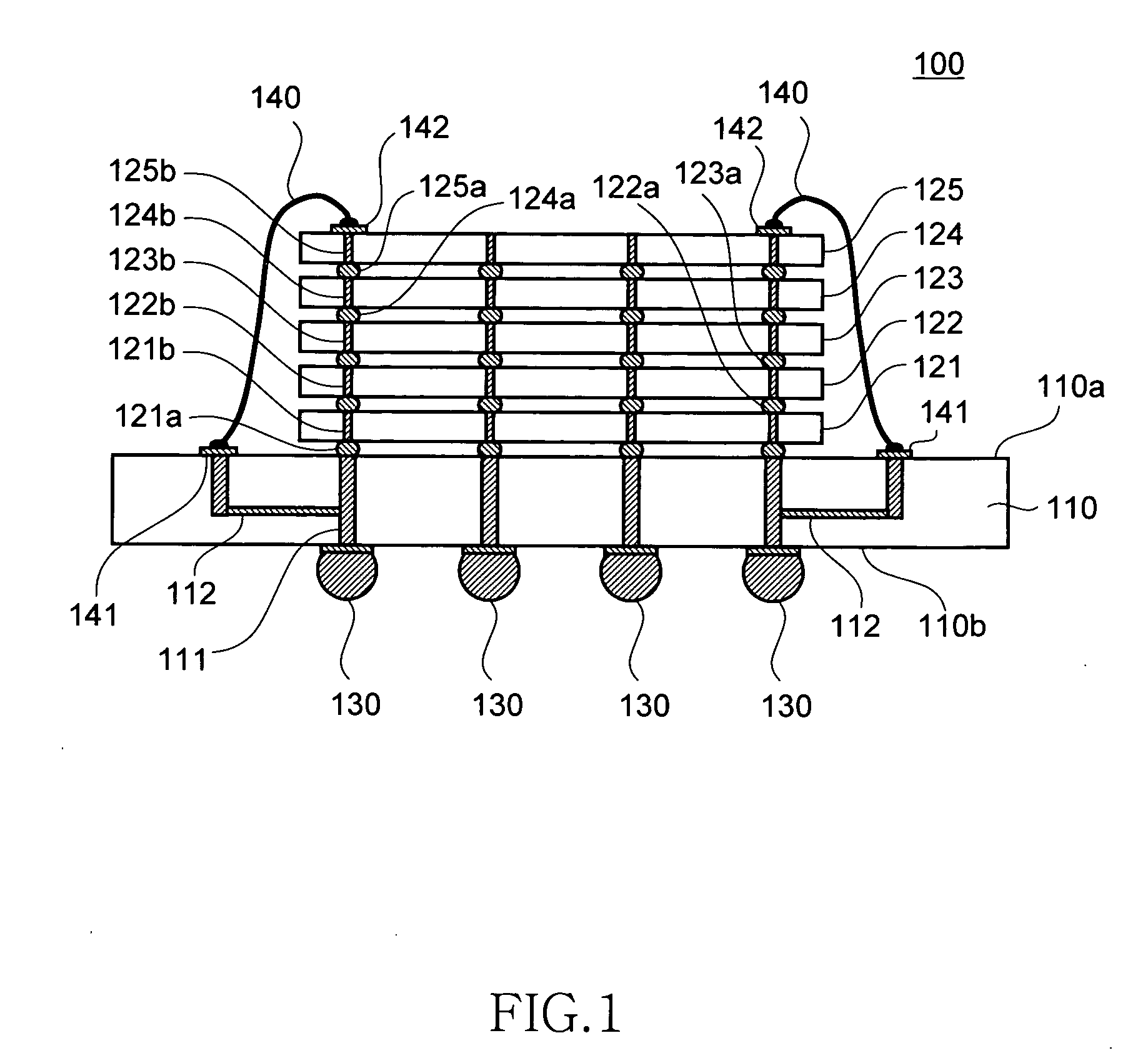
[0037]FIG. 1 is a schematic cross sectional view showing a structure of a stacked semiconductor device 100 according to a preferred first embodiment of the present invention.

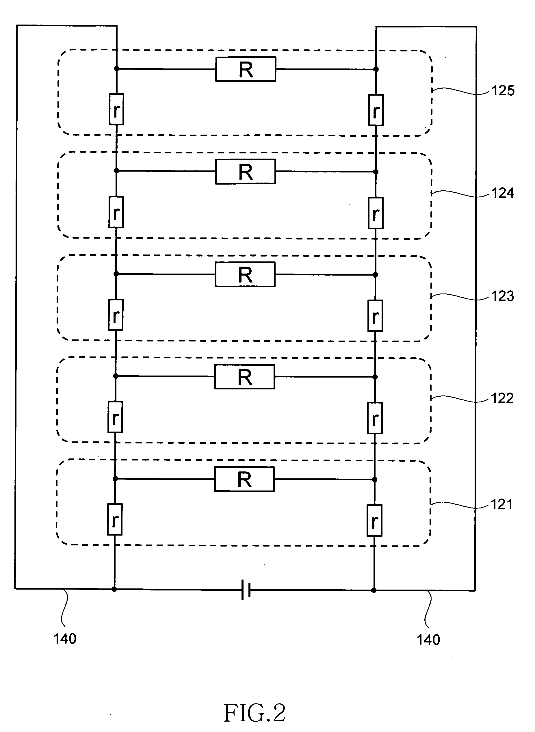
[0038]As shown in FIG. 1, the stacked semiconductor device 100 according to the present embodiment includes an interposer substrate 110, five semiconductor chips 121 to 125 stacked on one surface 110a of the interposer substrate 110, and external power supply terminals 130 arranged on the other surface 110b of the interposer substrate 110. While types of the semiconductor chips 121 to 125 are not particularly limited, core chips or interface chips, or the both chips can be used, when the stacked semiconductor device according to the embodiment is a DRAM. The number of stacked semiconductor chips is not limited to five, as long as it is two or more.

[0039]Besides the external power supply terminals 130, external signal terminals that input and output addresses, data, commands and the like are formed on the other s...

second embodiment

[0050]A stacked semiconductor device according to the present invention is explained next.

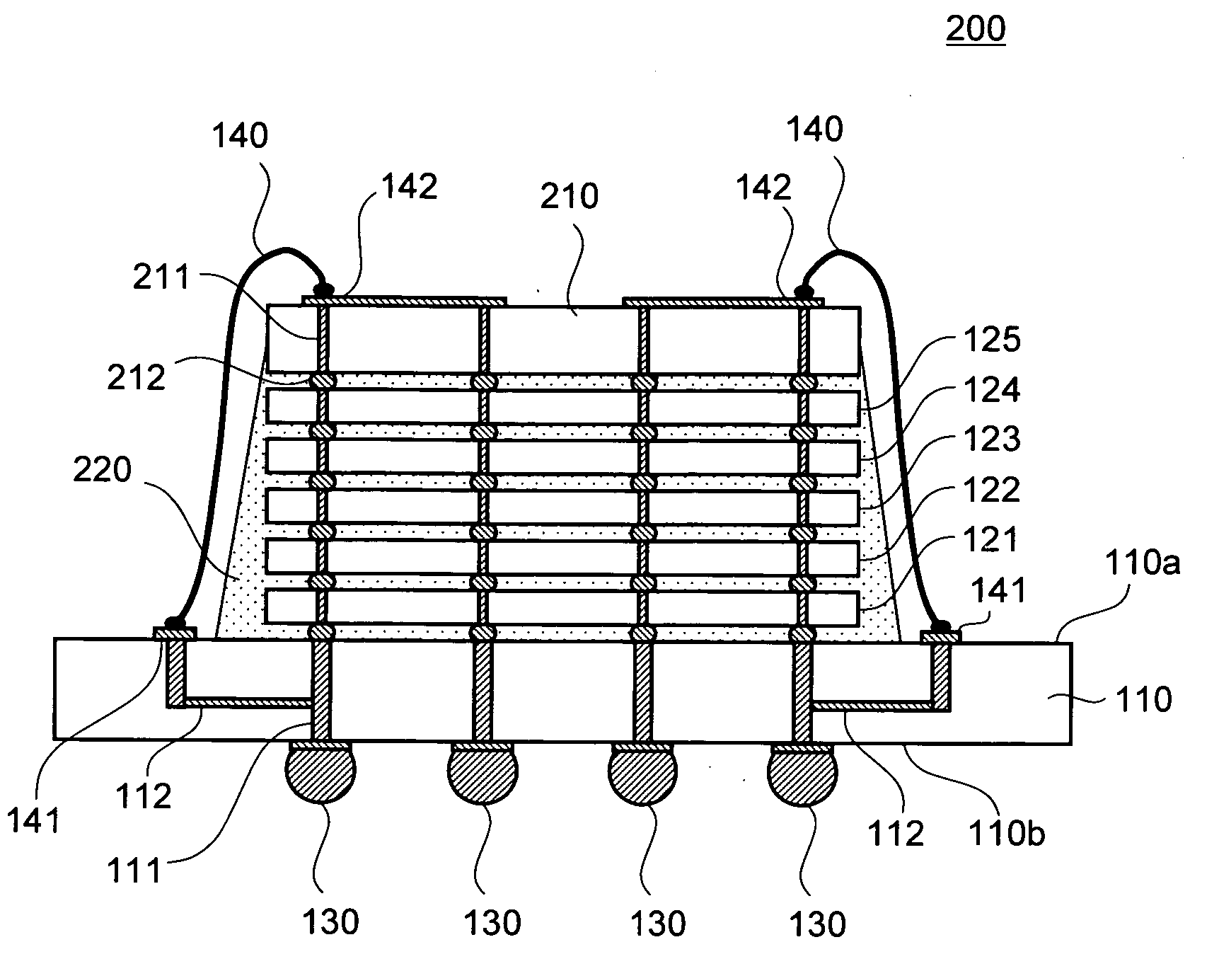
[0051]FIG. 3 is a schematic cross sectional view showing a structure of a stacked semiconductor device 200 according to the second embodiment.

[0052]As shown in FIG. 3, the stacked semiconductor device 200 according to the second embodiment is different from the stacked semiconductor device 100 according to the first embodiment in that a cap substrate 210 is arranged above the semiconductor chip 125 and an underfill material 220 is arranged between the interposer substrate 110 and the cap substrate 210. Since the rest of the configuration is basically the same as that of the stacked semiconductor device 100 according to the first embodiment, like parts are designated with like reference numerals, and redundant explanations will be omitted.

[0053]The cap substrate 210 serves to protect the semiconductor chips 121 to 125 from an impact generated at the time of bonding. That is, in the first embodim...

third embodiment

[0060]A stacked semiconductor device according to the present invention is explained next.

[0061]FIG. 5 is a schematic cross sectional view showing a structure of a stacked semiconductor device 300 according to the third embodiment.

[0062]As shown in FIG. 5, the stacked semiconductor device 300 according to the present embodiment is configured such that ten semiconductor chips 320 to 329 are stacked on the interposer substrate 110; a cap substrate 330 is arranged above the semiconductor chip 329 located in the top layer; and an intermediate interposer substrate 340 is arranged between lower-half five layers of the semiconductor chips 320 to 324 and upper-half five layers of the semiconductor chips 325 to 329.

[0063]The cap substrate 330 serves the same role as that of the cap substrate 210 used in the second embodiment. That is, the cap substrate 330 serves to lessen an impact generated at the time of wire bonding. The bonding wire 140 is connected to the bonding pad 142 arranged on th...


PUM


Abstract

A stacked semiconductor device includes an interposer substrate having external power supply terminals, and semiconductor chips stacked on the interposer substrate. A power supply wiring arranged in the semiconductor chip located in the bottom layer is connected to the external power supply terminal via a bump electrode, the power supply wiring arranged in the semiconductor chip located in the top layer is connected to the external power supply terminal via a bonding wire, and the power supply wirings each arranged in adjacent semiconductor chips are mutually connected via the through electrode. Such a loop structure can solve a problem such that the higher the semiconductor chip, the larger its voltage drop.

Description

TECHNICAL FIELD[0001]The present invention relates to a stacked semiconductor device. More specifically, the present invention relates to a stacked semiconductor device that can prevent a voltage drop in power source.BACKGROUND OF THE INVENTION[0002]In recent years, the storage density of semiconductor memory devices, represented by a DRAM (Dynamic Random Access Memory), has increased. It is increasingly demanded that these devices can operate at higher speeds. The increase in storage capacity has been achieved by making memory cells smaller and by increasing the chip size. However, the miniaturization of memory cells is physically limited, and the increase in chip size leads to a reduction of yield and impairs an increase of operating speed.[0003]To solve these problems fundamentally, there has been proposed a method such that a core unit having memory cells and an interface unit having peripheral circuits to the memory cells are provided as chips that are independent of each other...

Claims


Application Information

Patent Timeline
Patent Type & Authority Applications(United States)
IPC IPC(8): H01L23/02
CPCH01L24/73H01L2924/19107H01L2224/16225H01L2224/48091H01L2224/48227H01L2224/48464H01L2224/48465H01L2225/0651H01L2225/06513H01L2225/06517H01L2225/06527H01L2225/06555H01L2225/06572H01L2924/01029H01L2924/01079H01L2924/15184H01L2924/15192H01L2924/15311H01L25/0657H01L2224/16145H01L2224/14181H01L2224/13025H01L2924/01033H01L2924/01023H01L2924/01006H01L2924/00014H01L2924/00H01L2224/05573H01L2224/05647H01L2224/16146H01L2224/16235H01L2224/17181
Inventor ISHINO, MASAKAZUIKEDA, HIROAKIYAMADA, JUNJI
Owner MICRON TECH INC
Why Eureka
Try Eureka