Method and apparatus for scrubbing accumulated data errors from a memory system

Active Publication Date: 2010-12-30
TAIWAN SEMICON MFG CO LTD
View PDF27 Cites 58 Cited by
  • Summary
  • Abstract
  • Description
  • Claims
  • Application Information

AI Technical Summary

Benefits of technology

[0012]The data scrubbing apparatus may further suspend writing back during a writing of data to the array of memory cells. Additionall

Problems solved by technology

The data scrubbing apparatus receives an error indication that an error has occurred d

Method used


Image

  • Method and apparatus for scrubbing accumulated data errors from a memory system
  • Method and apparatus for scrubbing accumulated data errors from a memory system
  • Method and apparatus for scrubbing accumulated data errors from a memory system

Examples


Embodiment Construction

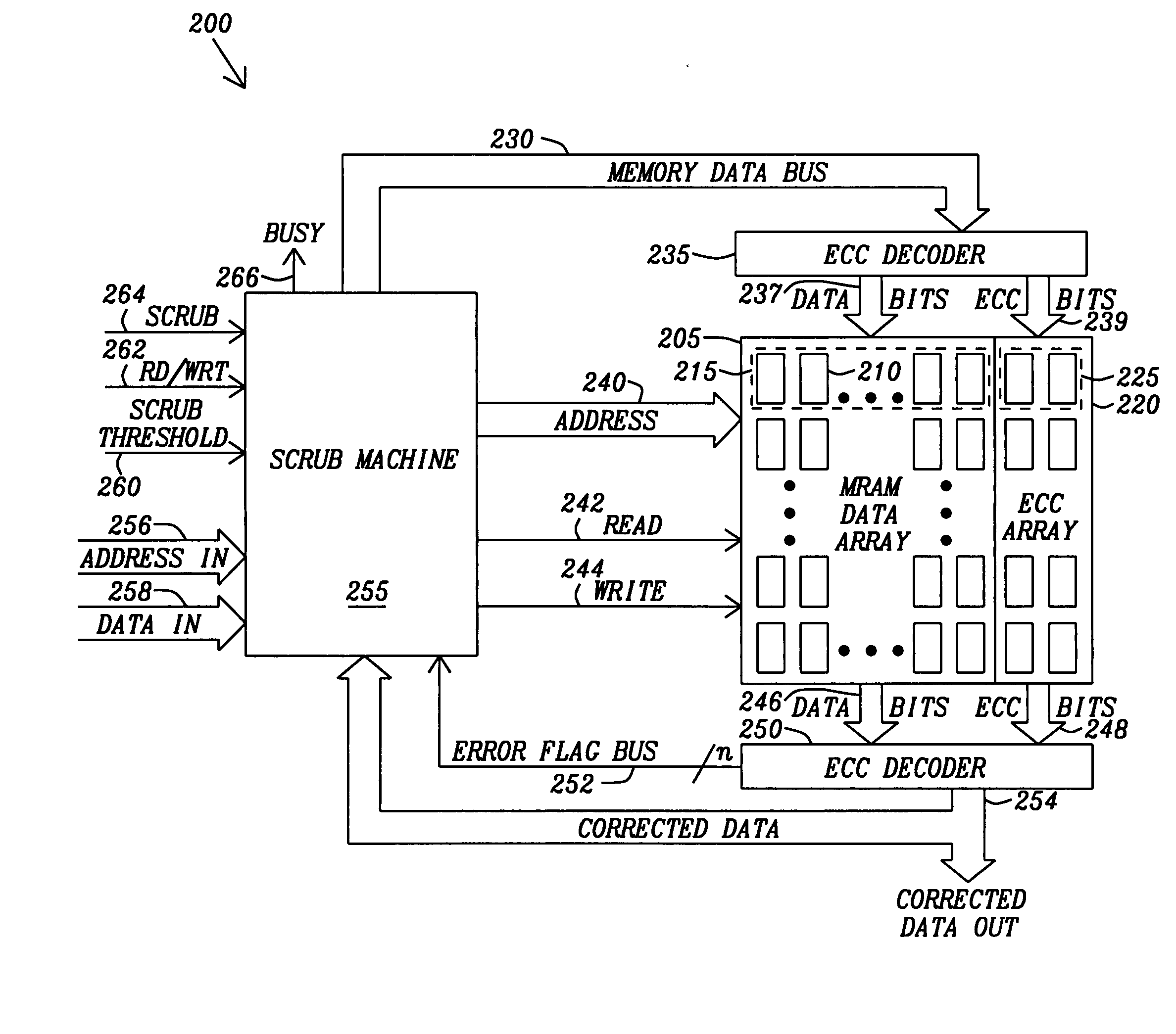
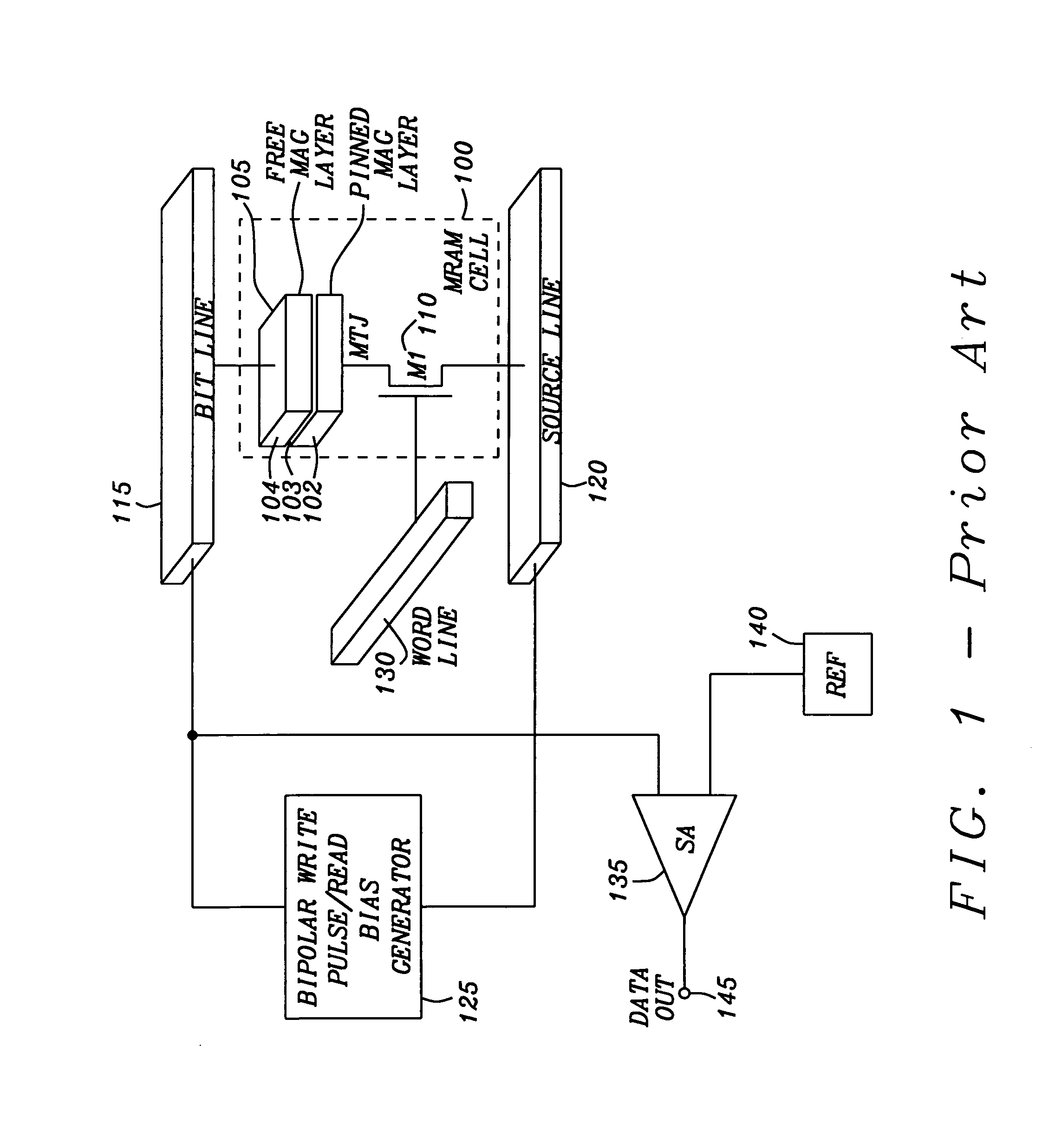
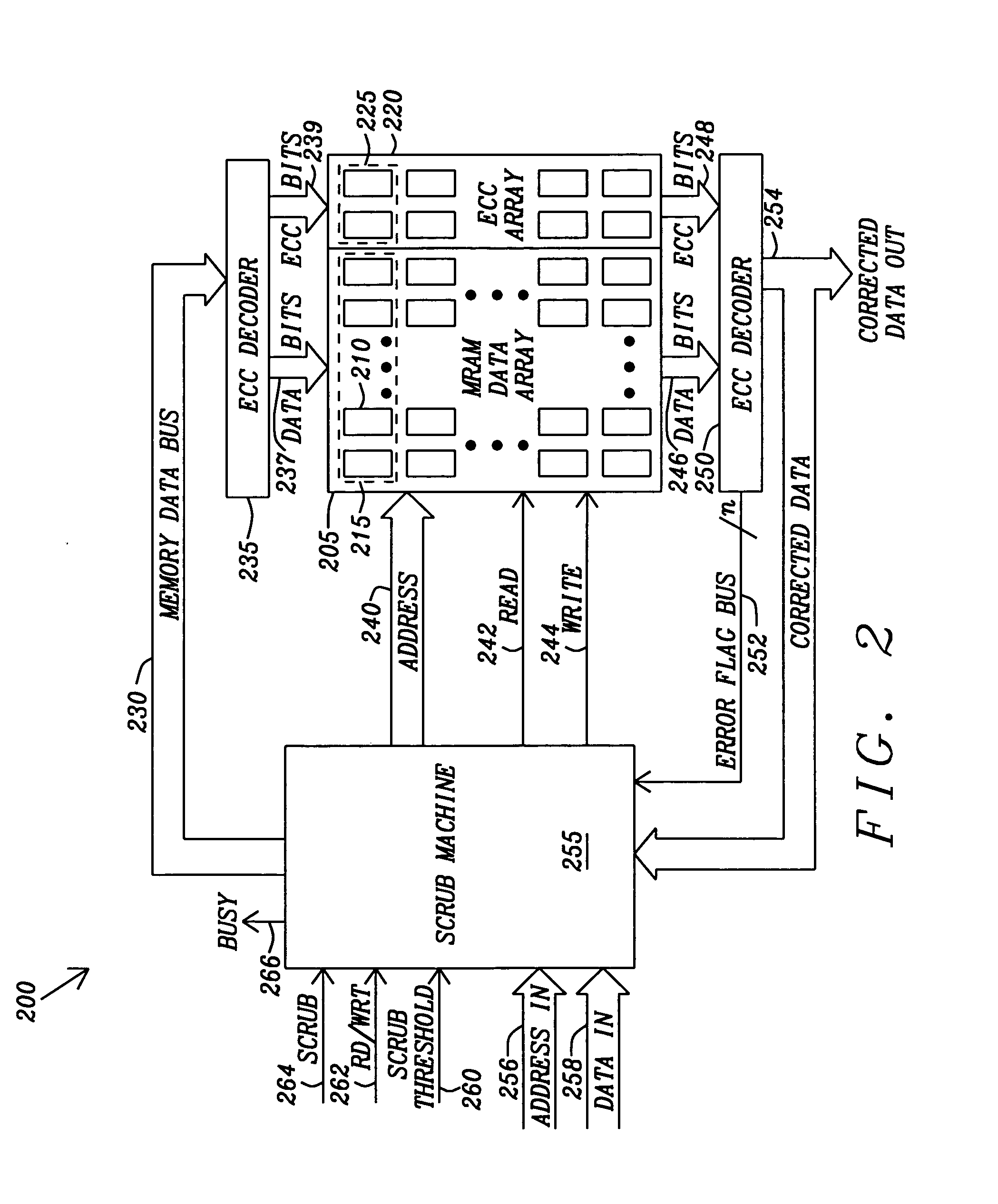
[0019]As illustrated in FIG. 1, a spin moment transfer (SMT) MRAM cell 100 consists of an MTJ element 105 and a Metal Oxide Semiconductor (MOS) transistor 110. The MTJ element 105 is composed of a pinned ferromagnetic layer 102 and a free ferromagnetic layer 104, and a tunnel barrier layer 103. The drain of the MOS transistor 110 is connected through a nonmagnetic layer to the pinned ferromagnetic layer 102. The free ferromagnetic layer 104 is connected to a bit line 115 and the source of the MOS transistor 110 is connected the source line 120. The bit line 115 and source select line 120 are connected to the bipolar write pulse / read bias generator 125. The bipolar write pulse / read bias generator 125 provides the necessary programming current to the MTJ element 105 through the bit line 115 and the source select line 120. The direction being determined by logic state being programmed to the MTJ element 105.

[0020]The gate of the MOS transistor 110 is connected to a word line 130. The w...


PUM


Abstract

A data scrubbing apparatus corrects disturb data errors occurring in an array of memory cells such as SMT MRAM cells. The data scrubbing apparatus receives an error indication that an error has occurred during a read operation of a grouping of memory cells within the array of memory cells. The data scrubbing apparatus may generate an address describing the location of the memory cells to be scrubbed. The data scrubbing apparatus then commands the array of memory cells to write back the corrected data. Based on a scrub threshold value, the data scrubbing apparatus writes the corrected data back after a specific number of errors. The data scrubbing apparatus may further suspend writing back during a writing of data. The data scrubbing apparatus provides a busy indicator externally during a write back of corrected data.

Description

BACKGROUND OF THE INVENTION[0001]1. Field of the Invention[0002]This invention relates generally to memory cells and array structures for memory cells. More particularly, this invention relates to magnetic random access memory (MRAM) cells and array structures for MRAM cells. Even more particularly, this invention relates to methods and apparatus for eliminating data errors in spin moment transfer (SMT) MRAM cells and array structures of spin moment transfer (SMT) MRAM cells.[0003]2. Description of Related Art[0004]The term Spin-RAM refers to a magnetic tunnel junction (MTJ) random access memory (RAM). In this context, the term “spin” refers to the angular momentum of electrons passing through an MTJ that will alter the magnetic moment of a free layer of an MTJ device. Electrons possess both electric charge and angular momentum (or spin). It is known in the art that a current of spin-polarized electrons can change the magnetic orientation of a free ferromagnetic layer of an MTJ via ...

Claims


Application Information

Patent Timeline
IPC IPC(8): G06F11/14G06F12/02
CPCG06F11/106
Inventor YANG, HSU KAI
Owner TAIWAN SEMICON MFG CO LTD
Why Eureka
Try Eureka