High voltage low power sensing device for flash memory

a sensing device and flash memory technology, applied in static storage, digital storage, instruments, etc., can solve the problems of limiting the potential level achieved by bit lines during sensing, current draw from external supply potentials, etc., to achieve lower voltage, reduce the potential level, and increase the operation potential.

Inactive Publication Date: 2005-07-05
MICRON TECH INC
View PDF17 Cites 2 Cited by
  • Summary
  • Abstract
  • Description
  • Claims
  • Application Information

AI Technical Summary

Benefits of technology

[0010]Single-ended sensing devices for sensing a programmed state of a floating-gate memory cell are described herein for use in high-voltage, low-power memory devices. Low-power memory devices rely on memory cells that operate at low voltages. However, some electronic systems may still provide higher supply potentials for operation of the memory device, e.g., 3V nominal. The drains of the memory cells must be protected from these higher supply potentials during sensing to avoid read disturb errors. One approach would be to provide a separate power supply, generated on-chip, to provide lower voltages during sensing. This approach, however, would result in a current draw from the external supply potential even during standby modes. The various embodiments of the invention provide protection of the memory cells from high external power supplies without the need to provide separate generation of lower potentials on-chip.
[0011]Sensing devices in accordance with the invention are adapted to accept supply potentials significantly higher than the maximum potential to be achieved on a bit line during a sensing operation. Sensing devices in accordance with the various embodiments include an input node selectively coupled to a floating-gate memory cell and an output node for providing an output signal indicative of the programmed state of the floating-gate memory cell. Such sensing devices further include a feedback loop coupled between a precharge path and the input node of the sensing device. The feedback loop limits the potential level achieved at the input node of the sensing device, thus limiting the potential level achieved by the bit lines during sensing.

Problems solved by technology

This approach, however, would result in a current draw from the external supply potential even during standby modes.
The feedback loop limits the potential level achieved at the input node of the sensing device, thus limiting the potential level achieved by the bit lines during sensing.

Method used


Image

  • High voltage low power sensing device for flash memory
  • High voltage low power sensing device for flash memory
  • High voltage low power sensing device for flash memory

Examples


Embodiment Construction

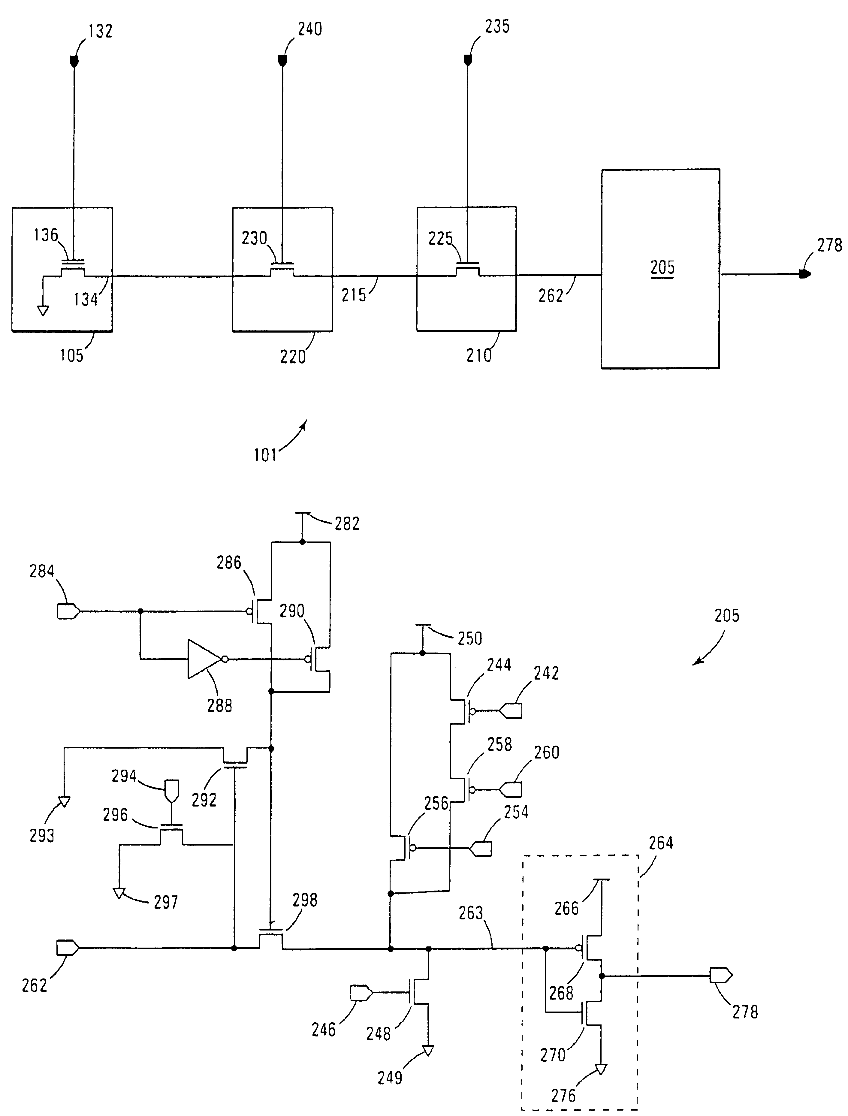
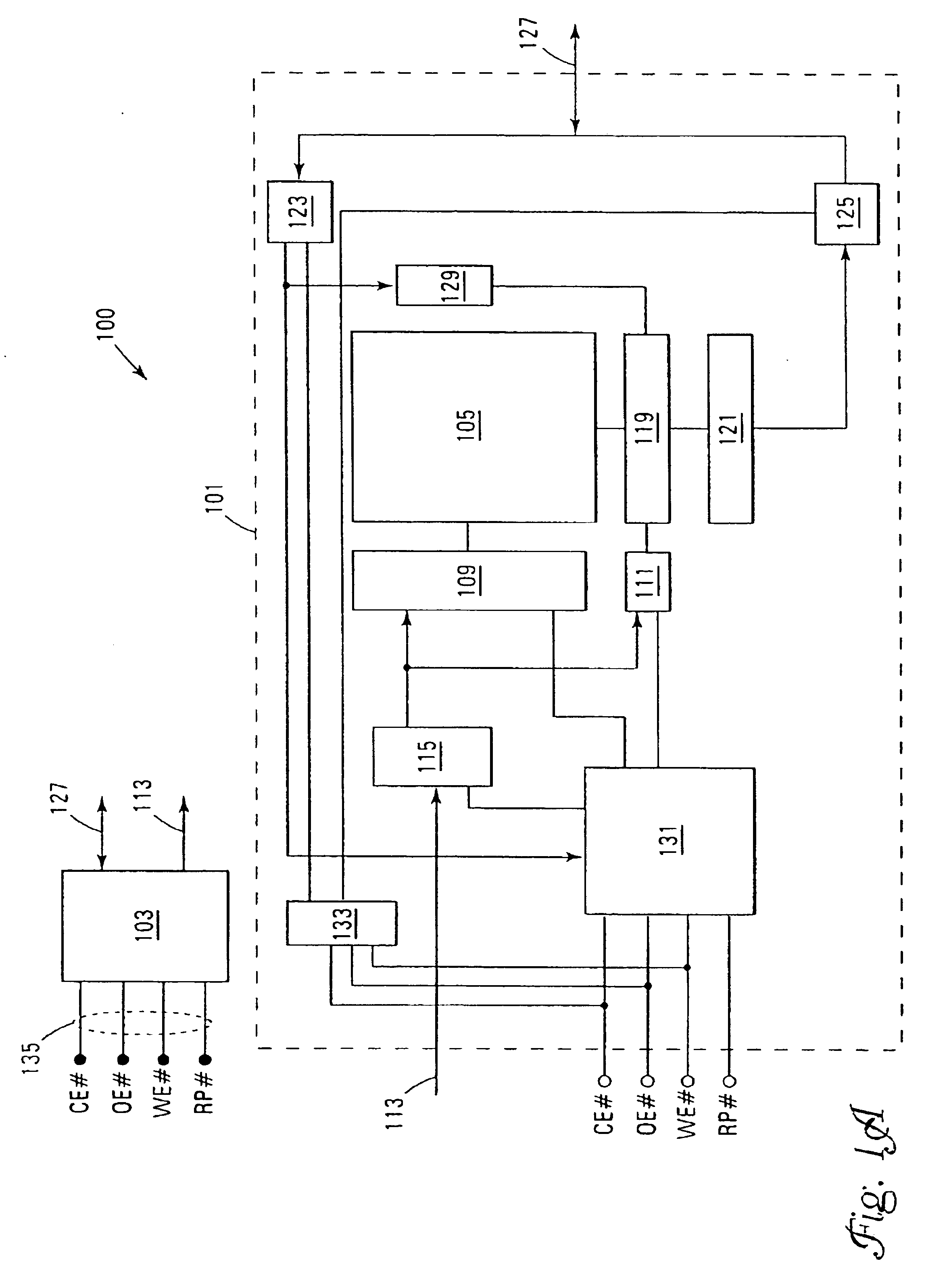
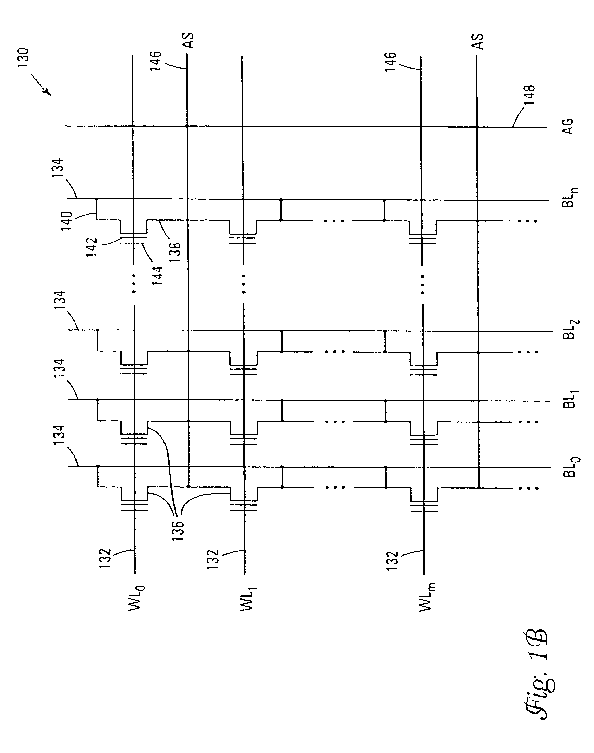
[0019]In the following detailed description of the present embodiments, reference is made to the accompanying drawings that form a part hereof, and in which is shown by way of illustration specific embodiments in which the inventions may be practiced. These embodiments are described in sufficient detail to enable those skilled in the art to practice the invention, and it is to be understood that other embodiments may be utilized and that process, electrical or mechanical changes may be made without departing from the scope of the present invention. The term substrate used in the following description includes any base semiconductor structure. Examples include silicon-on-sapphire (SOS) technology, silicon-on-insulator (SOI) technology, thin film transistor (TFT) technology, doped and undoped semiconductors, epitaxial layers of a silicon supported by a base semiconductor structure, as well as other semiconductor structures well known to one skilled in the art. Furthermore, when refere...


PUM


Abstract

Sensing devices for sensing a programmed state of a floating-gate memory cell are adapted for use in low-power memory devices using supply potentials that can be significantly higher than the maximum potential to be achieved on a local bit line during a sensing operation. Such sensing devices include an input node selectively coupled to a floating-gate memory cell and an output node for providing an output signal indicative of the programmed state of the floating-gate memory cell. Such sensing devices further include a feedback loop coupled between a precharge path and the input node of the sensing device. The feedback loop limits the potential level achieved at the input node of the sensing device, thus limiting the potential level achieved by the bit lines during sensing.

Description

RELATED APPLICATIONS[0001]This application is a continuation application of U.S. patent application Ser. No. 10 / 229,399 (allowed), filed Aug. 27, 2002 now U.S. Pat. No. 6,671,260, entitled “High Voltage Low Power Sensing Device For Flash Memory,” which application is commonly assigned and claims priority to Italian Patent Application Serial No. RM2001A000531, filed Aug. 31, 2001, entitled “High Voltage Low Power Sensing Device For Flash Memory.”[0002]This application is related to U.S. patent application Ser. No. 10 / 036,751 (allowed), filed Dec. 21, 2001, entitled “Sensing Scheme for Low-Voltage Flash Memory” and commonly assigned.TECHNICAL FIELD OF THE INVENTION[0003]The present invention relates generally to semiconductor memory devices, and in particular, the present invention relates to sensing schemes in semiconductor flash memory devices.BACKGROUND OF THE INVENTION[0004]Semiconductor memory devices are rapidly-accessible memory devices. In a semiconductor memory device, the ti...

Claims


Application Information

Patent Timeline
Patent Type & Authority Patents(United States)
IPC IPC(8): G11C7/06G11C16/26G11C16/06
CPCG11C7/062G11C7/067G11C16/26
Inventor VALI, TOMMASODE SANTIS, LUCA
Owner MICRON TECH INC
Why Eureka
Try Eureka