Multilayer wiring substrate

a wiring substrate and multi-layer technology, applied in the direction of printed circuit manufacturing, printed circuit aspects, printed electric component incorporation, etc., can solve the problems of substrate and warp amount delicately different, substrate warp is caused, and the strength of the multi-layer wiring substrate is inferior to the strength of the multi-layer wiring substrate itself, etc., to achieve suppressed warp of the substrate, high density, and high precision

Active Publication Date: 2011-01-06
SHINKO ELECTRIC IND CO LTD
View PDF13 Cites 29 Cited by
  • Summary
  • Abstract
  • Description
  • Claims
  • Application Information

AI Technical Summary

Benefits of technology

[0018]The insulating layers located adjacent to the center wiring layer on one side and the other side of the center wiring layer respectively may be formed of a resin material into which reinforcement is mixed, and the insulating layers located in outer layers than the insulating layers located adjacent to the center wiring layer may be formed of a resin material into which no reinforcement is mixed. Therefore, a warp of the substrate is suppressed effectively, and the wiring patterns formed in the multilayer wiring substrate can be formed with high precision and at a high density.
[0019]The insulating layers located in symmetrical positions with respect to the center wiring layer may be formed on one side and the other side of the center wiring layer such that stresses caused by the insulating layers formed on one side and the other side of the center wiring layer are made uneven, and the substrate may be planarized in which stresses caused by an uneven distribution of conductors in the wiring layers formed on one side and the other side of the center wiring layer are cancelled by the insulating layers. When the conductors of the wiring layers are distributed unevenly on one side and the other side of the center wiring layer, the insulating layers located in symmetrical positions with respect to the center wiring layer are formed such that the stresses caused due to the insulating layers are made uneven on one side and the other side of the center wiring layer. Therefore, a warp of the substrate can be suppressed, and the substrate can be made flat.
[0024]a plurality of vias, via which the wiring layers including the center wiring layer are connected electrically, wherein the via located on one side of the center wiring layer and the via located on the other side are formed in a symmetrical fashion with respect to the center wiring layer to have a trapezoidal sectional shape, a width of which is made narrower toward the center wiring layer, respectively. Therefore, a warp of the substrate due to the via arrangement can be reduced.
[0026]According to the present invention, such a multilayer wiring substrate can be provided that a stress of the substrate can be equalized on one side and the other side of the center wiring layer, a reduction in thickness of the substrate can be achieved, and a warp of the substrate can be prevented.

Problems solved by technology

However, the multilayer wiring substrate without the core substrate is inferior in strength of the substrate itself to the multilayer wiring substrate with the core substrate, and is ready to warp.
In this manner, arrangements of the conductor portions in respective layers are uneven, and as a result a warping direction (upward convex, downward convex, or the like) of the substrate and an amount of warp are delicately different.
In particular, in the multilayer wiring substrate without the core substrate, such a problem readily arises that, since strength of the substrate itself is insufficient, a warp of the substrate is caused due to a difference of balance such as a degree of shrinkage of the insulating layer, and the like.
Therefore, the stresses caused due to the insulating layers formed on one side and the other side of the center wiring layer can be made uneven.

Method used


Image

  • Multilayer wiring substrate
  • Multilayer wiring substrate
  • Multilayer wiring substrate

Examples


first embodiment

Multilayer Wiring Substrate

[0035]A first embodiment of a multilayer wiring substrate according to the present invention will be explained in detail with reference to the drawings hereinafter.

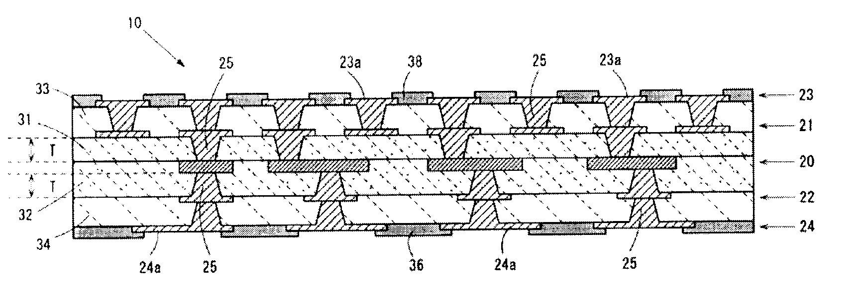
[0036]FIG. 1 is a sectional view showing a configuration of a first embodiment of a multilayer wiring substrate. A multilayer wiring substrate 10 of the present embodiment is constructed by stacking first, second, third, and fourth wiring layers 21, 22, 23, 24 on both sides of a center wiring layer 20 arranged at the center in the thickness direction of the substrate, while interposing insulating layers 31, 32, 33, 34 between these wiring layers. The multilayer wiring substrate 10 corresponds to the multilayer wiring substrate without the core substrate, which is equipped with four insulating layers and five wiring layers.

[0037]In FIG. 1, pads 23a to which a semiconductor element mounted on the multilayer wiring substrate 10 is connected are formed in the third wiring layer 23. Also, pads 24a to...

second embodiment

Multilayer Wiring Substrate

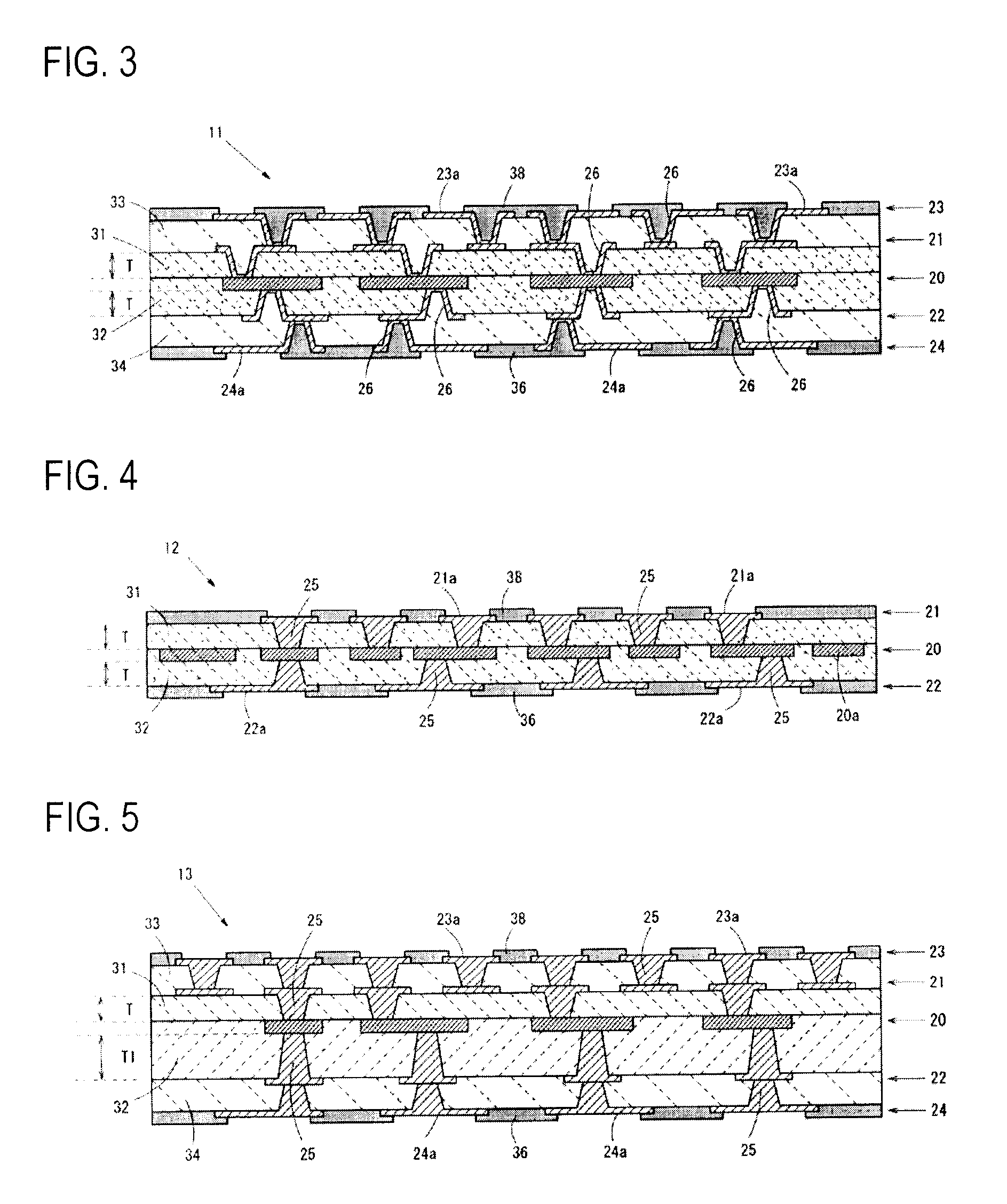
[0070]FIG. 5 shows a configuration of a second embodiment of the multilayer wiring substrate. In a multilayer wiring substrate 13, such a configuration is similar to the multilayer wiring substrate 10 shown in FIG. 1 that the wiring layers 21, 23 and the insulating layers 31, 33 are provided on one side of the center wiring layer 20 and also the wiring layers 22, 24 and the insulating layers 32, 34 are provided on the other side.

[0071]Also, it is similar to the first embodiment that the resin material of the same material quality is employed as the inner insulating layers 31, 32. A characteristic configuration of the multi layer wiring substrate 13 of the present embodiment resides in that a thickness of the insulating layer 32 on the other side is set thicker that a thickness of the insulating layer 31 on one side and thus the inner insulating layers 31, 32 are positively set to a different thickness respectively. In FIG. 5, the insulating layer 31 and th...


PUM


Abstract

A multilayer wiring substrate includes a center wiring layer arranged in a center of the substrate in a thickness direction, and wiring layers stacked on one side of the center wiring layer and the other side of the center wiring layer via an insulating layer. The wiring layers on one side of the center wiring layer and the wiring layers on the other side are provided in a same layer number. The insulating layers on one side of the center wiring layer and the insulating layers on the other side are provided in a same layer number.

Description

[0001]This application claims priority to Japanese Patent Application No. 2009-160134, filed Jul. 6, 2009, in the Japanese Patent Office. The Japanese Patent Application No. 2009-160134 is incorporated by reference in its entirety.TECHNICAL FIELD[0002]The present disclosure relates to a multilayer wiring substrate to which a warp preventing structure is provided.RELATED ART[0003]As a wiring substrate on which a semiconductor element is mounted, the multilayer wiring substrate in which a wiring layer is formed on both surfaces of a core substrate is widely employed. With a reduction in thickness of the multilayer wiring substrate and an increase in density of wiring patterns, the multilayer wiring substrate not equipped with a core substrate is provided nowadays. This multilayer wiring substrate without the core substrate possesses such advantages that a reduction in thickness is easy and wiring patterns can be formed with high density.[0004]However, the multilayer wiring substrate w...

Claims


Application Information

Patent Timeline
Patent Type & Authority Applications(United States)
IPC IPC(8): H05K1/14
CPCH05K3/025H05K3/108H05K3/4602H05K2203/1536H05K2201/0355H05K2203/0152H05K3/4652
Inventor SHOMURA, TOMOHIROIMASAKA, SHINICHI
Owner SHINKO ELECTRIC IND CO LTD
Why Eureka
Try Eureka