
Self-aligned wafer bonding

a self-aligned, wafer technology, applied in the direction of manufacturing tools, semiconductor/solid-state device details, natural mineral layered products, etc., can solve the problems of high precision alignment and difficult high precision alignmen

Active Publication Date: 2011-01-13
SEAGATE TECH LLC
View PDF5 Cites 22 Cited by
  • Summary
  • Abstract
  • Description
  • Claims
  • Application Information

AI Technical Summary

Benefits of technology

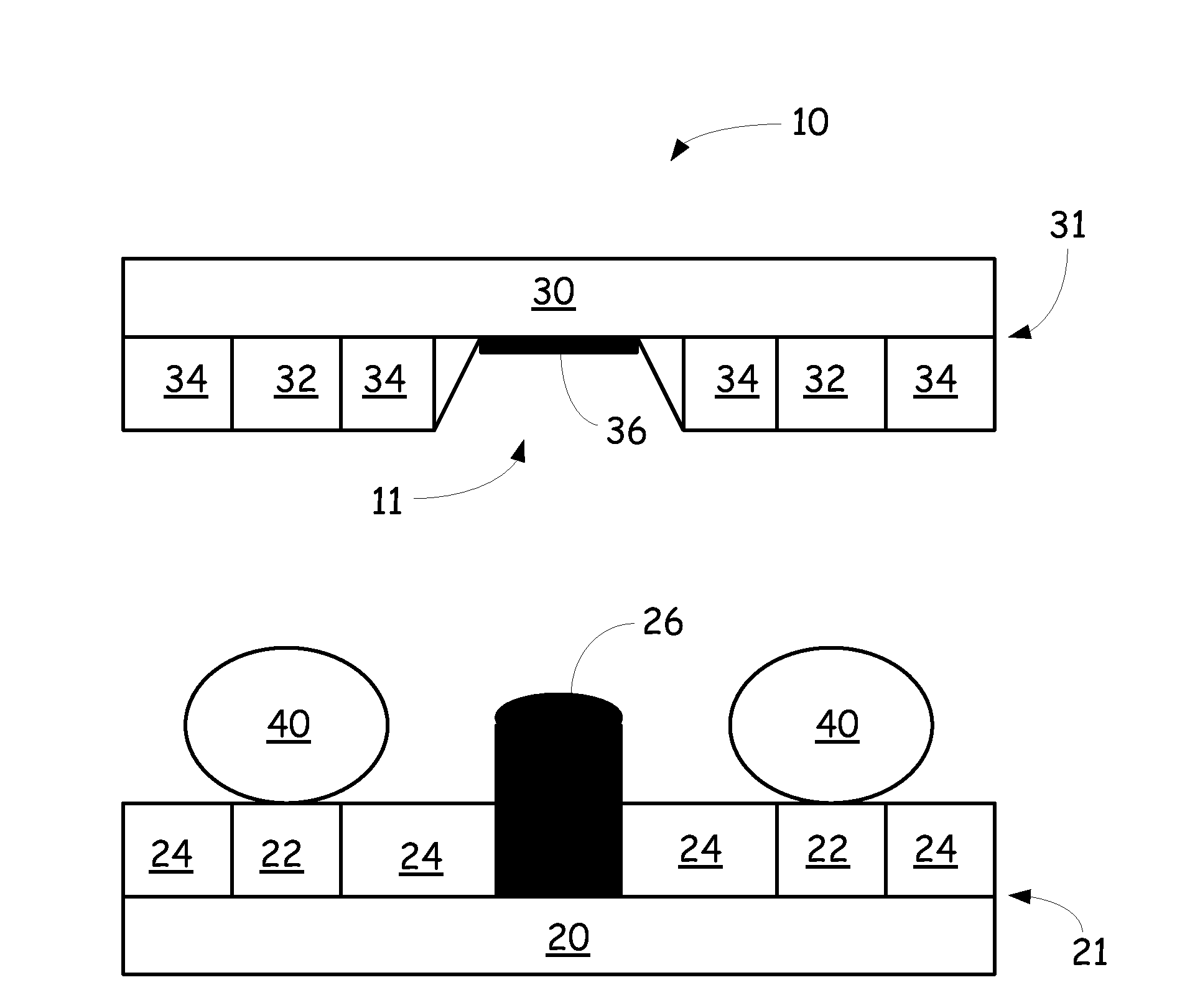
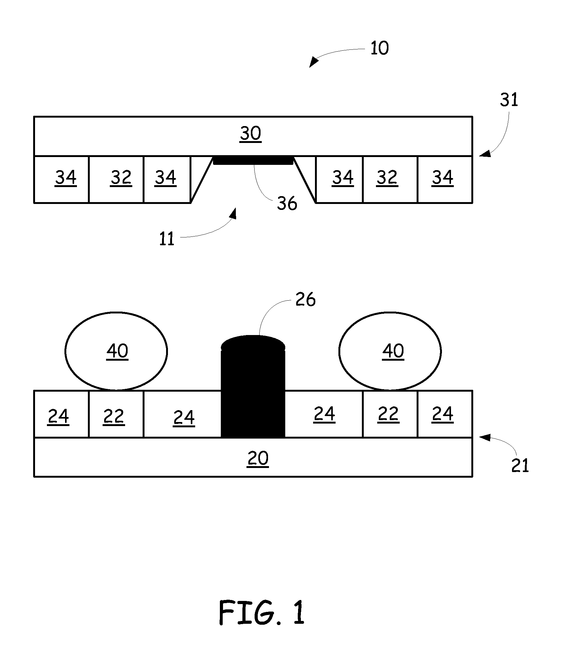
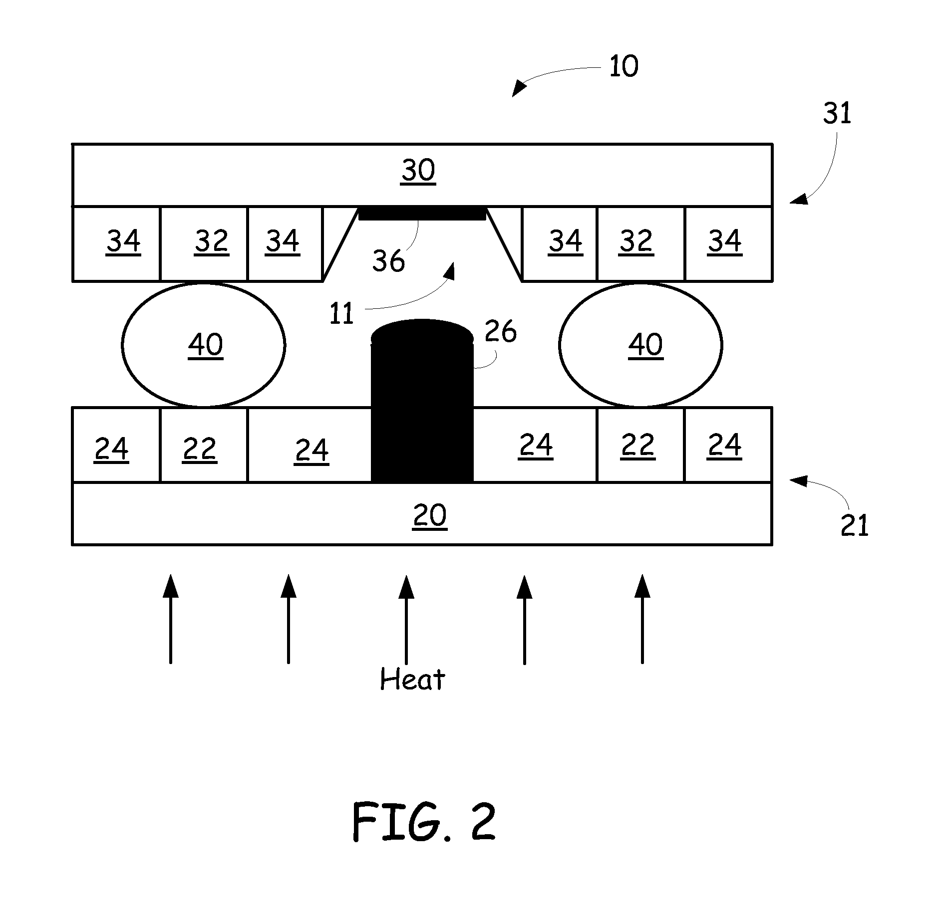
[0004]The present disclosure relates to self-aligned wafer bonding. In particular, the present disclosure relates to a self-alignment technique utilizing liquid surface tension to a

Problems solved by technology

However, when both of the wafers are opaque, high precision alignment is difficult.
As features scale down on the wafers, high precision alignment becomes more difficult.

Method used


Image

  • Self-aligned wafer bonding
  • Self-aligned wafer bonding
  • Self-aligned wafer bonding

Examples


Embodiment Construction

[0015]In the following description, reference is made to the accompanying set of drawings that form a part hereof and in which are shown by way of illustration several specific embodiments. It is to be understood that other embodiments are contemplated and may be made without departing from the scope or spirit of the present disclosure. The following detailed description, therefore, is not to be taken in a limiting sense. The definitions provided herein are to facilitate understanding of certain terms used frequently herein and are not meant to limit the scope of the present disclosure.

[0016]Unless otherwise indicated, all numbers expressing feature sizes, amounts, and physical properties used in the specification and claims are to be understood as being modified in all instances by the term “about.” Accordingly, unless indicated to the contrary, the numerical parameters set forth in the foregoing specification and attached claims are approximations that can vary depending upon the ...


PUM

PropertyMeasurementUnit
Nanoscale particle sizeaaaaaaaaaa
Pressureaaaaaaaaaa
Areaaaaaaaaaaa

Abstract

A wafer article includes a substrate, two or more hydrophilic areas disposed on the substrate, hydrophobic areas surrounding the hydrophilic areas, and a eutectic bonding material disposed on the substrate. A wafer apparatus including two wafers having complimentary hydrophilic regions and eutectic bonding material is disclosed and a method of forming a bonded wafer articles is disclosed.

Description

BACKGROUND[0001]Wafer to wafer, chip to wafer, or ship to chip (all used interchangeable herein) bonding can require high precision alignment and high precision bonding. Conventional precision alignment and bonding of wafers has consisted of visual alignment utilizing microscopes.[0002]Visual alignment can be useful when one of the wafers is transparent. However, when both of the wafers are opaque, high precision alignment is difficult. Conventional alignment techniques can have an alignment precision in a range from 5 to 10 micrometers.[0003]As features scale down on the wafers, high precision alignment becomes more difficult. There is a need for high precision wafer bonding technique that can align wafer features to within 100 nanometers or less.BRIEF SUMMARY[0004]The present disclosure relates to self-aligned wafer bonding. In particular, the present disclosure relates to a self-alignment technique utilizing liquid surface tension to align complimentary hydrophilic areas of two w...

Claims


Application Information

Patent Timeline
IPC IPC(8): B32B15/04B32B9/04B23K20/00B32B7/03
CPCH01L21/187Y10T428/24562H01L24/81H01L25/50H01L2224/0401H01L2224/05571H01L2224/13022H01L2224/131H01L2224/13147H01L2224/16111H01L2224/16147H01L2224/81001H01L2224/81143H01L2224/81191H01L2224/81203H01L2224/81385H01L2224/81805H01L2224/94H01L2225/06513H01L2924/01029H01L2924/01079H01L23/29Y10T428/24802Y10T428/24851Y10T428/24917H01L2924/0002H01L2924/00014B32B7/005B23K31/02H01L2924/01322H01L2924/0105H01L2924/01033H01L2224/05552H01L2224/81002Y10T428/31504Y10T428/31678B32B7/03
Inventor ZHENG, JUNSETIADI, DADI
Owner SEAGATE TECH LLC
Learn More