Low-pass filter, constant voltage circuit, and semiconductor integrated circuit including same

a constant voltage circuit and low-pass filter technology, applied in pulse techniques, oscillators, instruments, etc., can solve the problems of less successful implementation than desired, inapplicability of conventional low-pass filters, and drawbacks of low-pass filters b>210/b>

Active Publication Date: 2011-01-20
NISSHINBO MICRO DEVICES INC
View PDF6 Cites 30 Cited by
  • Summary
  • Abstract
  • Description
  • Claims
  • Application Information

AI Technical Summary

Benefits of technology

[0024]This disclosure describes an improved low-pass filter that filters an input signal input to a filter input terminal to output a filtered output signal to a filter output terminal.
[0025]In one aspect of the disclosure, the improved low-pass filter includes a capacitor, a first field-effect transistor, a first resistor, and a first current source. The capacitor is connected between the filter output terminal and ground. The first field-effect transistor has a gate terminal, a first conduction terminal connected to the filter input terminal, and a second conduction terminal connected to the filter output terminal. The first resistor is connected between the gate and first conduction terminals of the first transistor. The first current source is connected to the first resistor to supply a first current to the first resistor. The first resistor generates a first voltage thereacross based on the supplied first current for electrically biasing the gate terminal of the first transistor.
[0026]This disclosure also describes an improved constant voltage circuit that converts an input voltage input to a voltage input terminal to generate a constant output voltage output to a voltage output terminal.
[0027]In one aspect of the disclosure, the constant voltage circuit includes an output transistor, a reference voltage generator, a regulator control circuit, and a low-pass filter. The output transistor is connected between the voltage input and output terminals to control current flow therethrough according to a regulator control signal applied to a control terminal thereof. The reference voltage generator generates a reference voltage. The regulator control circuit is connected to the reference voltage generator and the voltage output terminal to generate the regulator control signal based on a comparison of the output voltage and the reference voltage for application to the control terminal of the output transistor. The low-pass filter has a filter input terminal connected to the reference voltage generator and a filter output terminal connected to the control circuit to filter the reference voltage input to the filter input terminal to output a filtered reference voltage to the filter output terminal. The low-pass filter includes a capacitor, a first field-effect transistor, a first resistor, and a first current source. The capacitor is connected between the filter output terminal and ground. The first field-effect transistor has a gate terminal, a first conduction terminal connected to the filter input terminal, and a second conduction terminal connected to the filter output terminal. The first resistor is connected between the gate and first conduction terminals of the first transistor. The first current source is connected to the first resistor to supply a first current to the first resistor. The first resistor generates a first voltage thereacross based on the supplied first current for electrically biasing the gate terminal of the first transistor.

Problems solved by technology

The conventional low-pass filter 110 is not practical where the cutoff frequency desired is very low.
Thus, the conventional low-pass filter 110 is implemented with at least one of the resistor R111 and the capacitor C111 built as a discrete component external from the integrated circuit, making the implementation less successful than desired.
Although effective in providing a low cutoff frequency with a relatively small circuit, the low-pass filter 210 depicted above has a drawback.
That is, variations in the cutoff frequency can occur due to variations in the impedance of the zero-biased transistor M211, which has variations in physical properties from one transistor to the next caused by manufacturing process inconsistencies or environmental changes that are difficult to control and eliminate completely, resulting in reduced accuracy and stability of the low-pass filter 210.

Method used


Image

  • Low-pass filter, constant voltage circuit, and semiconductor integrated circuit including same
  • Low-pass filter, constant voltage circuit, and semiconductor integrated circuit including same
  • Low-pass filter, constant voltage circuit, and semiconductor integrated circuit including same

Examples


Embodiment Construction

[0043]In describing exemplary embodiments illustrated in the drawings, specific terminology is employed for the sake of clarity. However, the disclosure of this patent specification is not intended to be limited to the specific terminology so selected, and it is to be understood that each specific element includes all technical equivalents that operate in a similar manner and achieve a similar result.

[0044]Referring now to the drawings, wherein like reference numerals designate identical or corresponding parts throughout the several views, examples and exemplary embodiments of this disclosure are described.

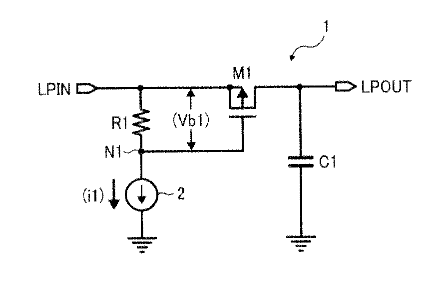
[0045]FIG. 5 is a circuit diagram schematically illustrating a low-pass filter 1 according to one embodiment of this patent specification.

[0046]As shown in FIG. 5, the low-pass filter 1 includes a first, p-channel metal-oxide semiconductor (PMOS) transistor M1, a capacitor C1, a first resistor R1 having a given resistance r1, and a first current source 2, which together form a fil...


PUM


Abstract

A low-pass filter that filters an input signal input to a filter input terminal to output a filtered output signal to a filter output terminal includes a capacitor, a first field-effect transistor, a first resistor, and a first current source. The capacitor is connected between the filter output terminal and ground. The first field-effect transistor has a gate terminal, a first conduction terminal connected to the filter input terminal, and a second conduction terminal connected to the filter output terminal. The first resistor is connected between the gate and first conduction terminals of the first transistor. The first current source is connected to the first resistor to supply a first current to the first resistor. The first resistor generates a first voltage thereacross based on the supplied first current for electrically biasing the gate terminal of the first transistor.

Description

BACKGROUND OF THE INVENTION[0001]1. Technical Field[0002]The present invention relates to a low-pass filter, a constant voltage circuit, and a semiconductor integrated circuit including the same, and more particularly, to a low-pass filter and a constant voltage circuit for use in ultra-low noise constant voltage regulation which can be integrally formed on a single semiconductor substrate, and a semiconductor integrated circuit including such a voltage regulator with a low-pass filter incorporated therein.[0003]2. Discussion of the Background[0004]Electronic low-pass filters are used in various semiconductor circuits which eliminate high frequencies above a given cutoff frequency to provide accurate signals free from high-frequency noise. One typical application is in voltage regulation, where a low-pass filter is connected between a reference voltage generator output terminal and a regulator output terminal to filter out flicker or 1 / f noise inherent in the semiconductor device fr...

Claims


Application Information

Patent Timeline
Patent Type & Authority Applications(United States)
IPC IPC(8): G05F3/02H04B1/00
CPCG05F1/575
Inventor AISU, KATSUHIKO
Owner NISSHINBO MICRO DEVICES INC
Why Eureka
Try Eureka