Methods for fabricating non-planar semiconductor devices having stress memory

a non-planar semiconductor and stress memory technology, applied in semiconductor/solid-state device manufacturing, basic electric elements, electric devices, etc., can solve the problem of increasing the carrier mobility, excessively difficult implementation of conventional straining techniques, and achieving a fraction (e.g., approximately half) of the carrier mobility

Inactive Publication Date: 2011-02-03
ALSEPHINA INNOVATIONS INC
View PDF5 Cites 25 Cited by
  • Summary
  • Abstract
  • Description
  • Claims
  • Application Information

AI Technical Summary

Benefits of technology

[0005]Embodiments of a method are provided for fabricating a non-planar semiconductor device including a substrate having a plurality of raised crystalline structures formed thereon. In one embodiment, the method includes the steps of amorphorizing a portion of each raised crystalline structure included within the plurality of raised crystalline structures, forming a sacrificial strain layer over the plurality of raised crystalline structures to apply stress to the amorphized portion of each raised crystalline structure, annealing the non-planar semiconductor device to recrystallize the amorphized portion of each raised crystalline structure in a stress-memorized state, and removing the sacrificial strain layer.

Problems solved by technology

However, the unique topography of FinFETs and other non-planar semiconductor devices (e.g., triFETs) generally renders the implementation of conventional straining techniques excessively difficult.
Even when it is practicable to utilize strain layers during the fabrication of a non-planar semiconductor device, any increase in carrier mobility improvement is typically limited; e.g., due to the lack of a confined source / drain, deposition of strained SiGe is predicted to result in a fraction (e.g., approximately half) of the carrier mobility achieved when similar straining techniques are utilized in conjunction with planar MOSFETs.

Method used


Image

  • Methods for fabricating non-planar semiconductor devices having stress memory
  • Methods for fabricating non-planar semiconductor devices having stress memory
  • Methods for fabricating non-planar semiconductor devices having stress memory

Examples


Embodiment Construction

[0009]The following Detailed Description is merely exemplary in nature and is not intended to limit the invention or the application and uses of the invention. Furthermore, there is no intention to be bound by any expressed or implied theory presented in the preceding Technical Field, Background, Brief Summary, or the following Detailed Description.

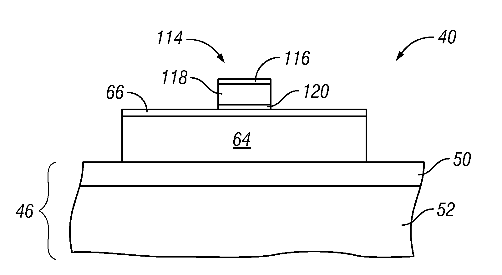
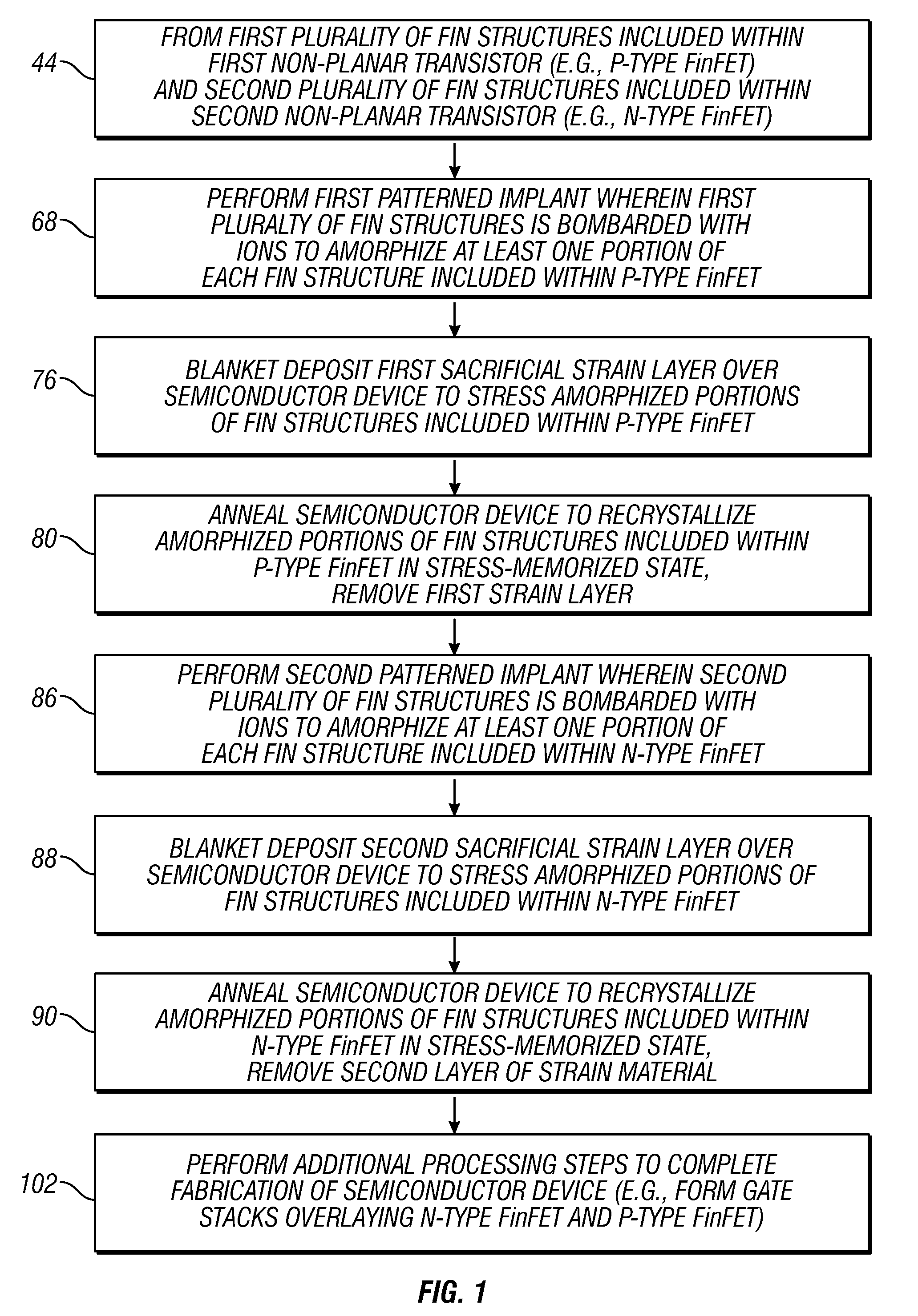
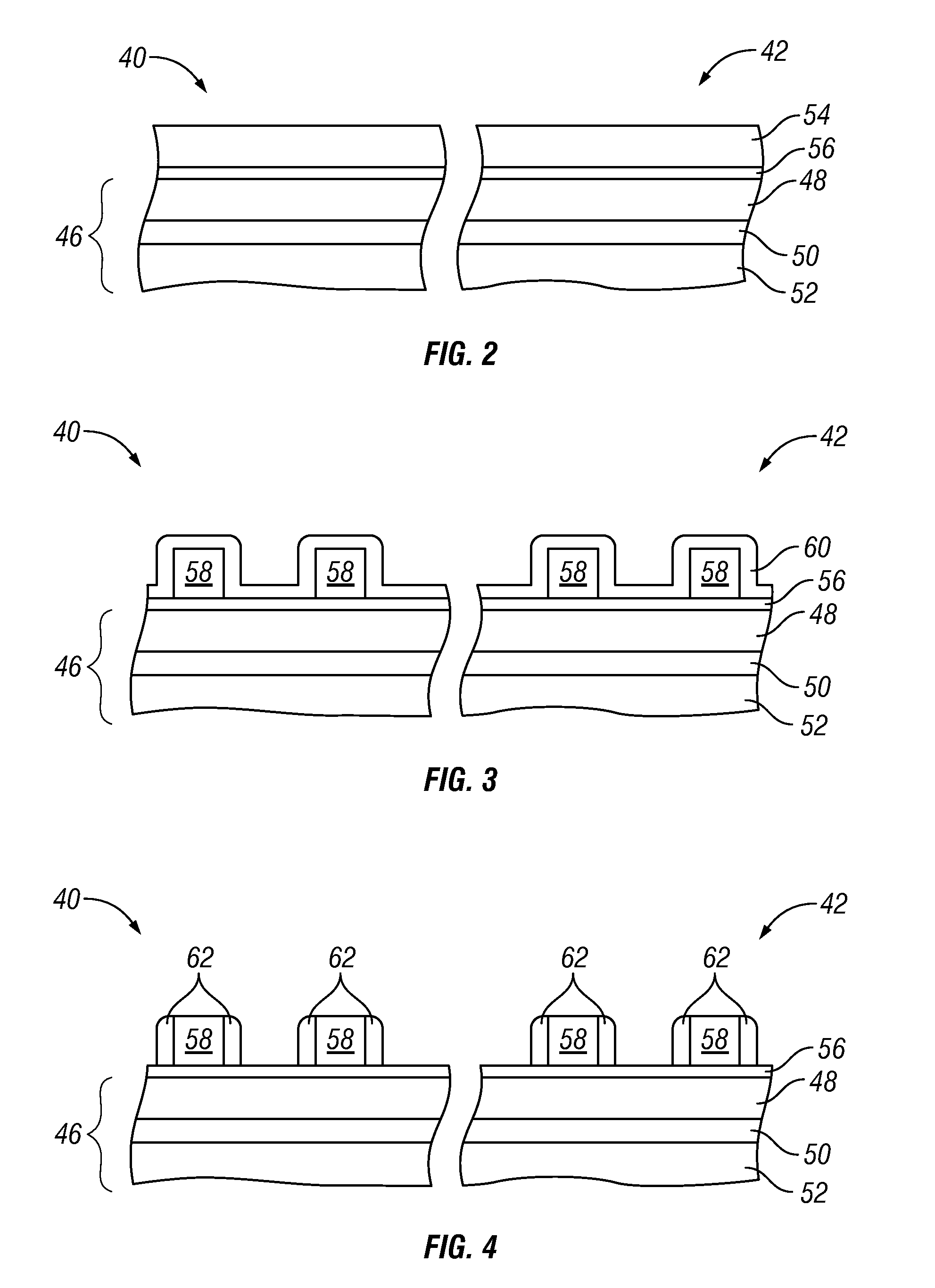
[0010]FIG. 1 is a flowchart illustrating an exemplary method for fabricating a non-planar semiconductor device in which stress memory is imparted to one or more raised crystalline structures, such as a plurality of fin structures. By way of non-limiting illustration, the exemplary method shown in FIG. 1 is described below in conjunction with an exemplary semiconductor device 40, 42 including two complementary non-planar transistors, namely, a P-type FinFET 40 and an N-type FinFET 42. FIGS. 2-16, also described below, are simplified cross-sectional views of semiconductor device 40, 42 illustrating P-type FinFET 40 and N-type FinFET 42 at v...


PUM

PropertyMeasurementUnit
thicknessaaaaaaaaaa
thicknessaaaaaaaaaa
grazing anglesaaaaaaaaaa

Abstract

Embodiments of a method are provided for fabricating a non-planar semiconductor device including a substrate having a plurality of raised crystalline structures formed thereon. In one embodiment, the method includes the steps of amorphorizing a portion of each raised crystalline structure included within the plurality of raised crystalline structures, forming a sacrificial strain layer over the plurality of raised crystalline structures to apply stress to the amorphized portion of each raised crystalline structure, annealing the non-planar semiconductor device to recrystallize the amorphized portion of each raised crystalline structure in a stress-memorized state, and removing the sacrificial strain layer.

Description

TECHNICAL FIELD[0001]The present invention relates generally to non-planar semiconductor devices and, more particularly, to embodiments of a method for fabricating a non-planar semiconductor device wherein stress memory is imparted to one or more raised crystalline structures (e.g., fin structures) included within the non-planar semiconductor device.BACKGROUND[0002]In contrast to conventional planar metal-oxide-semiconductor field-effect transistors (“MOSFETs”), multi-gate transistors incorporate two or more gates into a single device. Relative to single gate transistors, multi-gate transistors reduce off-state current leakage, increase on-state current flow, and reduce overall power consumption. Multi-gate devices having non-planar topographies also tend to be more compact than conventional planar transistors and consequently permit higher device densities to be achieved. One known type of non-planar, multi-gate transistor, commonly referred to as a “FinFET,” includes at least one ...

Claims


Application Information

Patent Timeline
Patent Type & Authority Applications(United States)
IPC IPC(8): H01L21/26H01L21/28
CPCH01L21/26586H01L29/66795H01L29/66803H01L29/785H01L29/7847
Inventor HARGROVE, MICHAEL J.JOHNSON, FRANK SCOTTLUNING, SCOTT
Owner ALSEPHINA INNOVATIONS INC
Why Eureka
Try Eureka