Information processing device

a technology of information processing and processing device, which is applied in the direction of electric digital data processing, instruments, computing, etc., can solve the problem that the initialization of the device cannot be performed

Active Publication Date: 2011-02-03
LAPIS SEMICON CO LTD
View PDF6 Cites 77 Cited by
  • Summary
  • Abstract
  • Description
  • Claims
  • Application Information

AI Technical Summary

Problems solved by technology

However, there are cases where initialization of the device cannot be performed by resetting the device.

Method used


Image

  • Information processing device
  • Information processing device
  • Information processing device

Examples


first embodiment

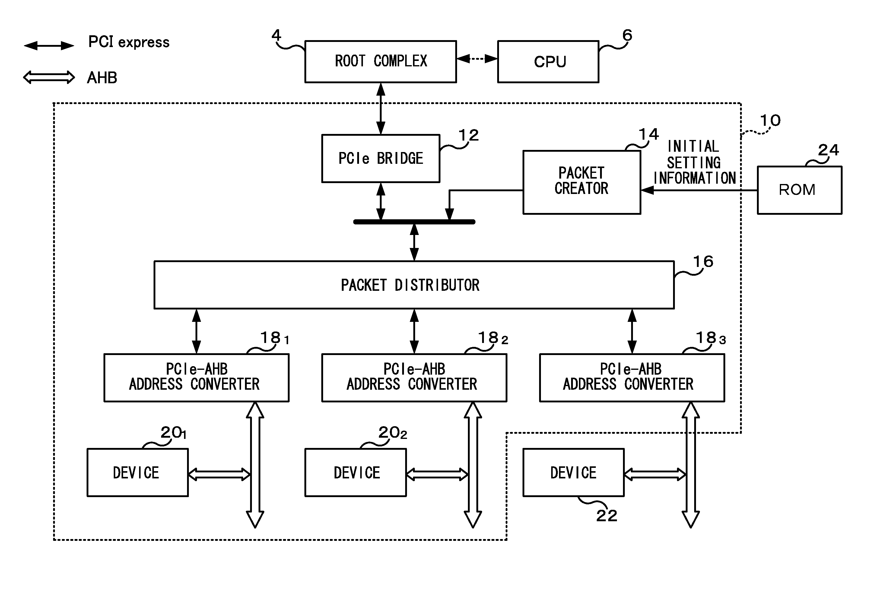
[0037]FIG. 1 shows one example of the general configuration of an information processing device 10 of a The information processing device 10 of the present embodiment is, as one example, formed on one chip (not shown).

[0038]In the present embodiment, there will be described a case where the information processing device 10 is, as one specific example, an information processing device for using devices 201 and 202 connected to an AHB bus and a device 22 as devices connected to a PCIe bus. As one specific example, it will be assumed that the devices 201 and 202 are devices that have unique identification addresses such as MAC addresses, for example, and that the devices 201 and 202 are devices that are unaware of those unique identification addresses. As one specific example, it will be assumed that the device 22 is a programmable device such as a FPGA and is a device having a unique address width and an offset address (an address dependent on an internal memory address).

[0039]The in...

second embodiment

[0083]For example, like in a second embodiment shown in FIG. 11, the information processing device may also be configured like an information processing device 50 that performs initial setting when it uses, as devices connected to a PCIe bus, devices having unique identification addresses connected to a non-PCIe bus. In this case, devices 201 to 203 are all devices having unique identification addresses. In a ROM 54, for example, only initial setting information that generates the initialization setting packet when AE=01 or 10 is stored beforehand. An initialization setting packet creator 52 corresponding to the packet creator 14 creates and outputs only the initialization setting packet. PCIe-AHB address converters 561 to 563 have the general configuration shown in FIG. 12.

third embodiment

[0084]For example, like in a third embodiment shown in FIG. 13, the information processing device may also be configured like an information processing device 60 that performs initial setting when it uses, as devices connected to a PCIe bus, device having unique PCIe address widths and AHB offset addresses connected to a non-PCIe bus. In this case, devices 221 to 223 are all devices having unique PCIe address widths and AHB offset addresses. In a ROM 64, for example, only initial setting information that generates the change setting packet when AE=01 or 10 is stored beforehand. An initial change setting packet creator 62 corresponding to the packet creator 14 creates and outputs only the change setting packet. PCIe-AHB address converters 661 to 663 have the general configuration shown in FIG. 16.

[0085]As described above, in the information processing device 10 of the present embodiment, the packet creator 14 reads the initial setting information stored beforehand in the ROM 24 at th...


PUM


Abstract

An information processing device includes: an address converter including a base address register in which address conversion information is stored and a conversion circuit that converts a PCI Express standard bus address of an inputted packet to a non-PCI Express standard bus address; and a packet generator. When first configuration information of a first device that has a device-unique unique address, is connected to a non-PCI Express standard bus and is unaware of the unique address is stored, the packet generator generates an address setting-use configuration write request packet, and when second configuration information including change information for changing the base address register to a base address register of a second device where at least one of an address width and an internal memory address is a device-unique unique value, the packet generator generates a change setting-use configuration write request packet and outputs the generated packet to the address converter.

Description

CROSS-REFERENCE TO RELATED APPLICATION[0001]This application claims priority under 35 USC 119 from Japanese Patent Application No. 2009-175706 filed on Jul. 28, 2009, the disclosure of which is incorporated by reference herein.BACKGROUND OF THE INVENTION[0002]1. Field of the Invention[0003]The present invention relates to an information processing device for performing information exchange by a PCI Express bus and a non-PCI Express bus interface.[0004]2. Description of the Related Art[0005]In recent years, an I / O serial interface called PCI Express has been used in personal computers (PCs) and associated peripherals.[0006]PCI Express (hereinafter abbreviated as “PCIe”) realizes a 2-Gbps transfer speed by using 1 lane and realizes a 64-Gbps transfer speed by using 32 lanes.[0007]In PCIe, there are prescribed layer structures resulting from the three layers of a physical layer, a data link layer and a transaction layer (see FIG. 2) and the two layers of a software layer and a configur...

Claims


Application Information

Patent Timeline
Patent Type & Authority Applications(United States)
IPC IPC(8): G06F3/00
CPCG06F2213/0026G06F13/387
Inventor UEHARA, TERUAKI
Owner LAPIS SEMICON CO LTD
Why Eureka
Try Eureka