LED module and lighting device using the same

a technology of led modules and lighting devices, applied in the direction of final product manufacturing, with built-in power, sustainable manufacturing/processing, etc., can solve the problems of difficult to attach the surface mounting type led package to the lighting device, and the size of the surface mounting type led package is small, so as to achieve the effect of narrowing the distan

Active Publication Date: 2011-02-10
PANASONIC CORP
View PDF21 Cites 35 Cited by
  • Summary
  • Abstract
  • Description
  • Claims
  • Application Information

AI Technical Summary

Benefits of technology

[0009]In this case, it is possible to obtain the LED module having a desired shape by cutting the LED package wafer along the groove. In addition, each the surface mounting type LED package is spaced from adjacent the surface mounting type LED package by a width of the groove. Therefore, it is possible to narrow the distance between each one of the surface mounting type LED packages and the other of the surface mounting type LED packages.
[0010]It is preferred that the flexible wiring substrate is provided with an electrical insulation substrate, a first penetration wiring, and a second penetration wiring. The electrical insulation substrate has flexibility. The patterned wiring is disposed in an internal portion of the electrical insulation substrate. The first penetration wiring is formed in the internal portion of the electrical insulation substrate so as to electrically connect the first connection electrode to the patterned wiring. The second penetration wiring is formed in the internal portion of the electrical insulation substrate so as to electrically connect the second connection electrode with the patterned wiring.

Problems solved by technology

However, the surface mounting type LED package is very small.
Therefore, it is difficult to attach the surface mounting type LED package to the lighting device having a various shape in high density.

Method used


Image

  • LED module and lighting device using the same
  • LED module and lighting device using the same
  • LED module and lighting device using the same

Examples


first embodiment

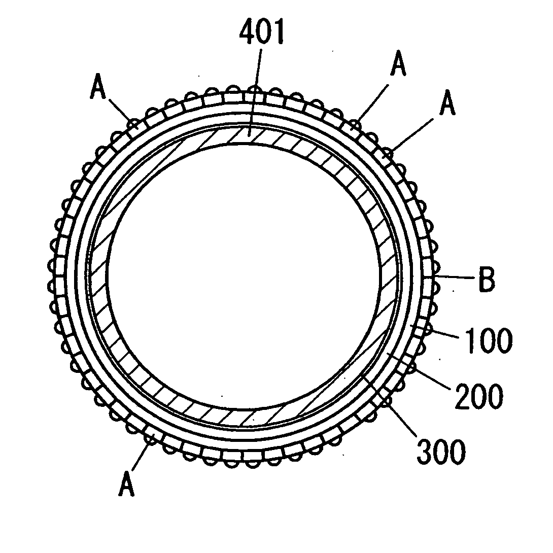
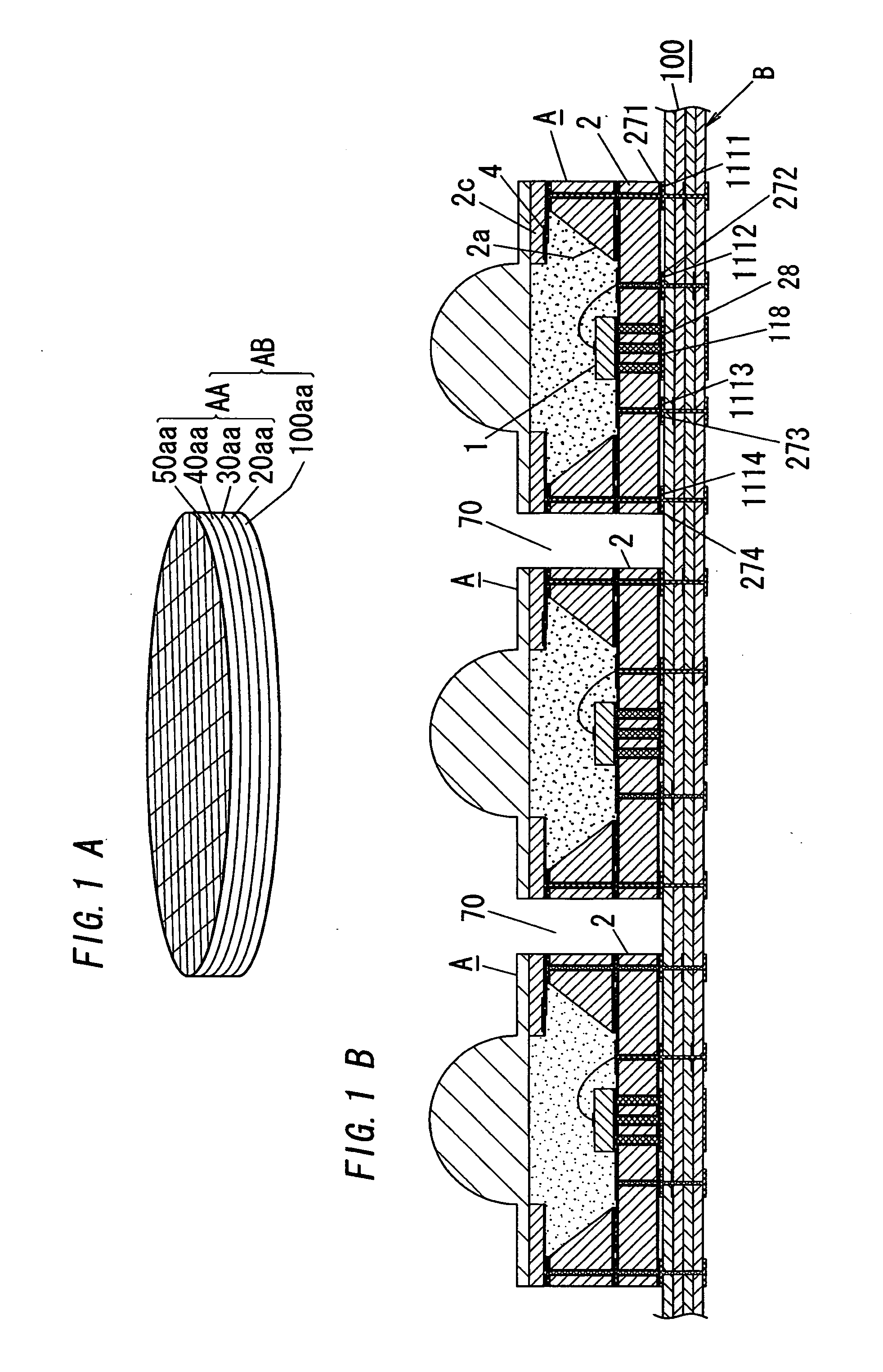
[0075]An explanation of an LED module in the first embodiment of this invention is made with attached Figs. FIG. 1 B shows a side cross sectional view of the LED module B in this embodiment. FIG. 2 shows a part of side cross sectional view of the LED module in this embodiment. Each FIG. 1 B and FIG. 2 shows the LED module B of this embodiment comprising a flexible wiring substrate 100 and a plurality of surface mounting type LED packages A. A plurality of surface mounting type LED packages A are disposed on an upper surface of the flexible wiring substrate 100.

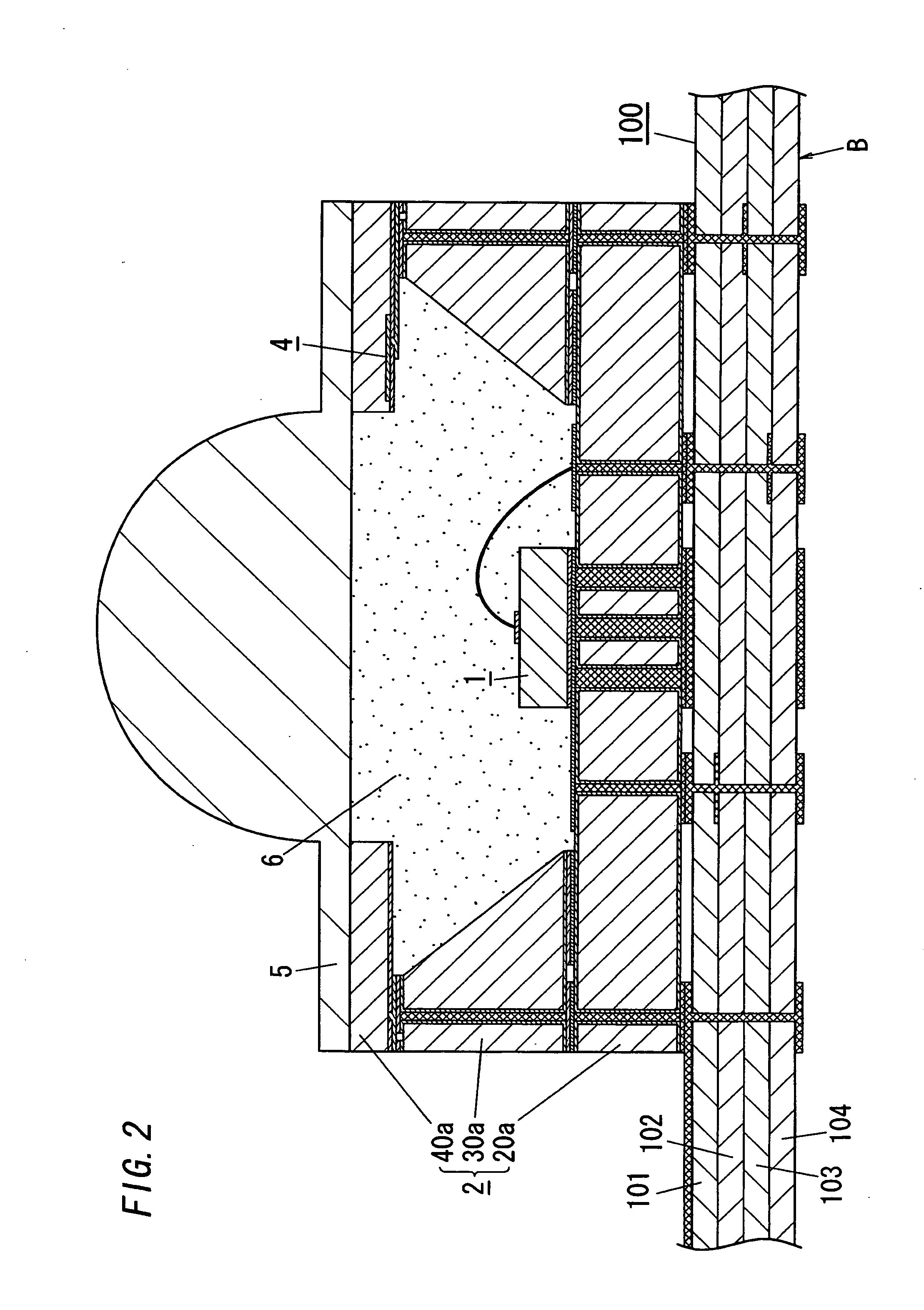
[0076]FIG. 3 shows a side cross sectional view taken along the line of X-Y. As shown in FIG. 3, the surface mounting type LED package A comprises a mounting substrate 2, an LED chip 1, a sealing material 6, a cover 5, and wirings. Each the wiring is made of metal.

[0077]The mounting substrate 2 comprises a base 20, a spacer 30, and a frame 40. A base 20 is made from a silicone substrate 20a. The silicone substrate 20a is provid...

second embodiment

[0112]The LED module B in the second embodiment is explained with attached drawings. It should be noted that the components in common with the components of the first embodiment is symbolized by the same reference numerals. Therefore, explanations of the components in common with the components of the first embodiment are omitted.

[0113]FIG. 9 shows an LED module B in this embodiment. The LED module B in this embodiment comprises the flexible wiring substrate 100 and the surface mounting type LED package AP.

[0114]The surface mounting type LED package AP comprises a mounting substrate 2, the LED chip 1, the sealing material 6, the cover 5, the wirings, and the electrical current regulation circuit substrate 60.

[0115]The electrical current regulation circuit substrate 60 is made of silicon. The electrical current regulation circuit substrate 60 is provided at its front surface and its rear surface with an electrical insulation film which is not shown in the drawing. The electrical curr...

third embodiment

[0123]The LED module in the third embodiment of this invention is explained with attached drawings. It is noted that the components in common with the components of the first embodiment and the second embodiment is symbolized by the same reference numerals. Therefore, the explanation of the components in common with the components of the first embodiment and the second embodiment is omitted. As shown in FIG. 11, the LED module B in this embodiment comprises a surface mounting type LED package AQ and a flexible wiring substrate 10.

[0124]The surface mounting type LED package AQ comprises a mounting substrate 2, an LED chip 1, a sealing material 6, a cover 5, and wirings.

[0125]The mounting substrate 2 comprises a base 20, a spacer 30, and a frame 40B. The frame 40B is disposed on an upper surface of the spacer 30. The frame 40B is formed at is center with an aperture 41. The aperture 41 penetrates through the frame 40B in the thickness direction of the frame 40B. The frame 40B is provi...


PUM


Abstract

The LED module comprises a flexible wiring substrate and surface mounting type LED packages. The flexible wiring substrate is formed at its surface with power supply terminals which comprises a first electrode pad and a second electrode pad, and is formed with a patterned wiring being electrically connected to the patterned wiring. The surface mounting type LED package comprises an LED chip and a mounting substrate. The mounting substrate is formed at its front surface with a recess, and its rear surface with a first connection electrode and the second connection electrode which are electrically connected to the first electrode pad and the second electrode pad, respectively when the mounting substrate is mounted on the flexible wiring substrate. The LED chip is disposed within the recess so as to receive the electrical current through the outside connection electrode and the power supply terminal.

Description

TECHNICAL FIELD[0001]This invention relates to an LED module and a lighting device using the LED module.BACKGROUND ART[0002]Japanese patent application publication No. 2005-327820A discloses a prior art surface mounting type LED package. The surface mounting type LED package comprises an LED chip, a mounting substrate, and a cover. The mounting substrate is made from a semiconductor substrate. The semiconductor substrate is provided at its top surface with a recess. The LED chip is disposed in the recess. The cover is made of glass. The cover is attached to the mounting substrate such that the cover covers an opening of the recess.[0003]In the prior art surface mounting type LED package, the mounting substrate is provided at its bottom surface with a pair of patterned electrical conductor. Each the patterned electrical conductor is electrically connected to each electrode of the LED chip. In addition, the mounting substrate is formed at its rear surface with a pair of external conne...

Claims


Application Information

Patent Timeline
Patent Type & Authority Applications(United States)
IPC IPC(8): H01L31/14H01L33/08F21S2/00F21S8/04F21S9/02F21S9/03F21Y101/02H01L33/48H01L33/58H01L33/60H01L33/62
CPCF21S4/003F21Y2101/02H01L2924/3025H01L2924/10253H05K2201/10106H05K1/189H05K1/181H01L33/486H01L33/58H01L33/642H01L2224/48091H05K1/0287H05K1/0298H05K1/112H01L2924/00014H01L2924/00F21S4/20F21Y2115/10H01L24/97H01L2224/48227H01L2224/73265H01L2924/181Y02P70/50H01L2924/00012
Inventor KIRIHARA, MASAOHOSHINO, KANAKO
Owner PANASONIC CORP
Why Eureka
Try Eureka