Method Of Reducing Bit Error Rate For A Flash Memory

a flash memory and bit error rate technology, applied in the field of flash memory, can solve the problems of error bits, error correction control (ecc) may not be able to correct error bits, threshold voltage distribution may shift, etc., and achieve the effect of reducing the coupling

Active Publication Date: 2011-02-17
JIANGSU HUACUN ELECTRONICS TECH CO LTD
View PDF10 Cites 36 Cited by
  • Summary
  • Abstract
  • Description
  • Claims
  • Application Information

AI Technical Summary

Benefits of technology

[0008]In view of the foregoing, it is an object of the present embodiment to provide a method of bit error rate for a flash memory in order to cancel or at least reduce the coupling effect between neighboring pages of the flash memory.

Problems solved by technology

In practice, however, the threshold voltage distribution may probably shift after the flash memory has been subjected to a predetermined number of program / erase cycles or / and a predetermined data retention time has elapsed.
Furthermore, due to coupling effect caused by neighboring page or pages, the distribution may widen sufficiently such that neighboring states may partially overlap.
Furthermore, the neighboring states of the shifted distribution 12 partially overlap, resulting in error bits.
If the extent of the overlapping is large, error correction control (ECC) may not be capable of correcting the error bits.

Method used


Image

  • Method Of Reducing Bit Error Rate For A Flash Memory
  • Method Of Reducing Bit Error Rate For A Flash Memory
  • Method Of Reducing Bit Error Rate For A Flash Memory

Examples


Embodiment Construction

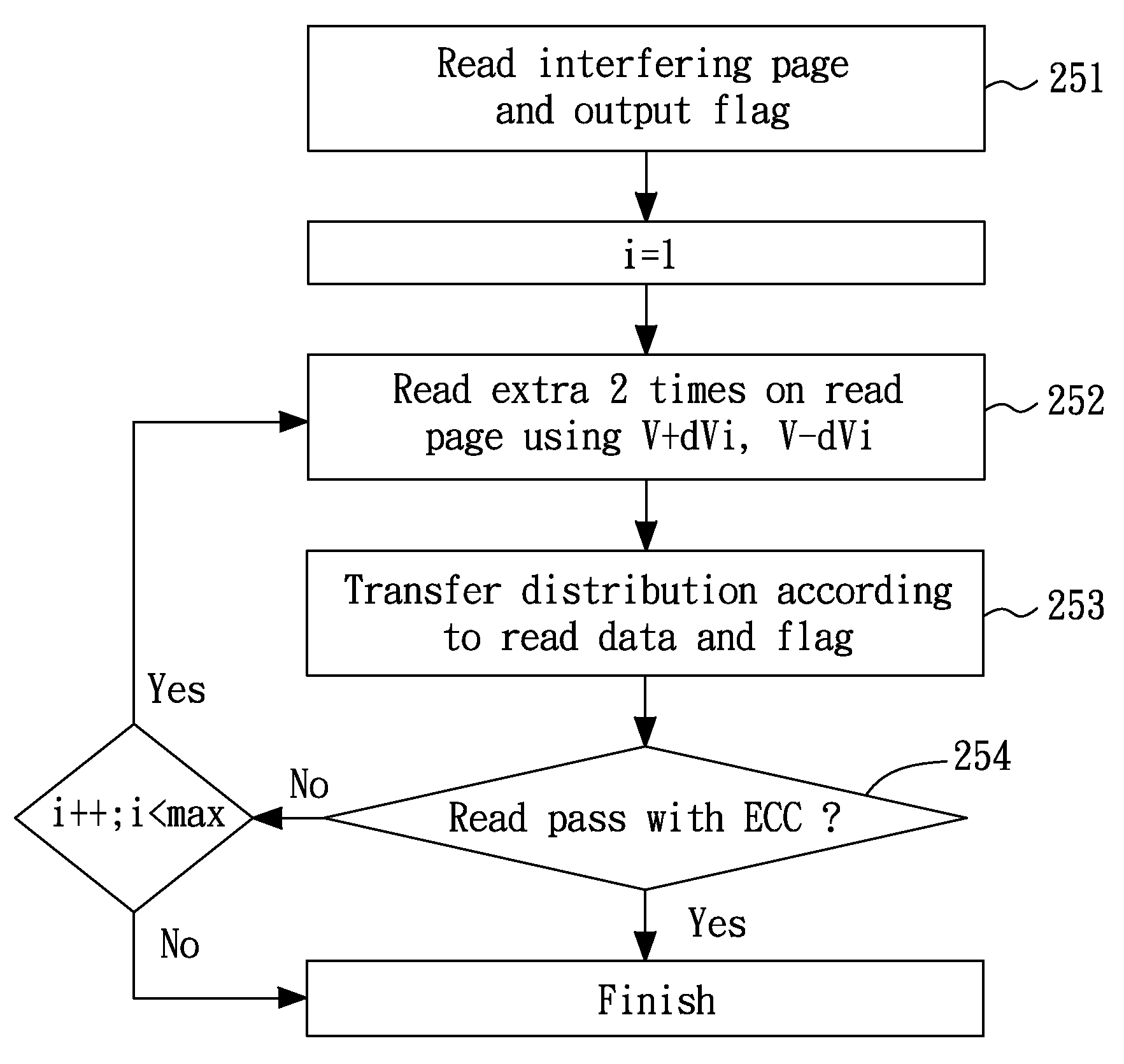
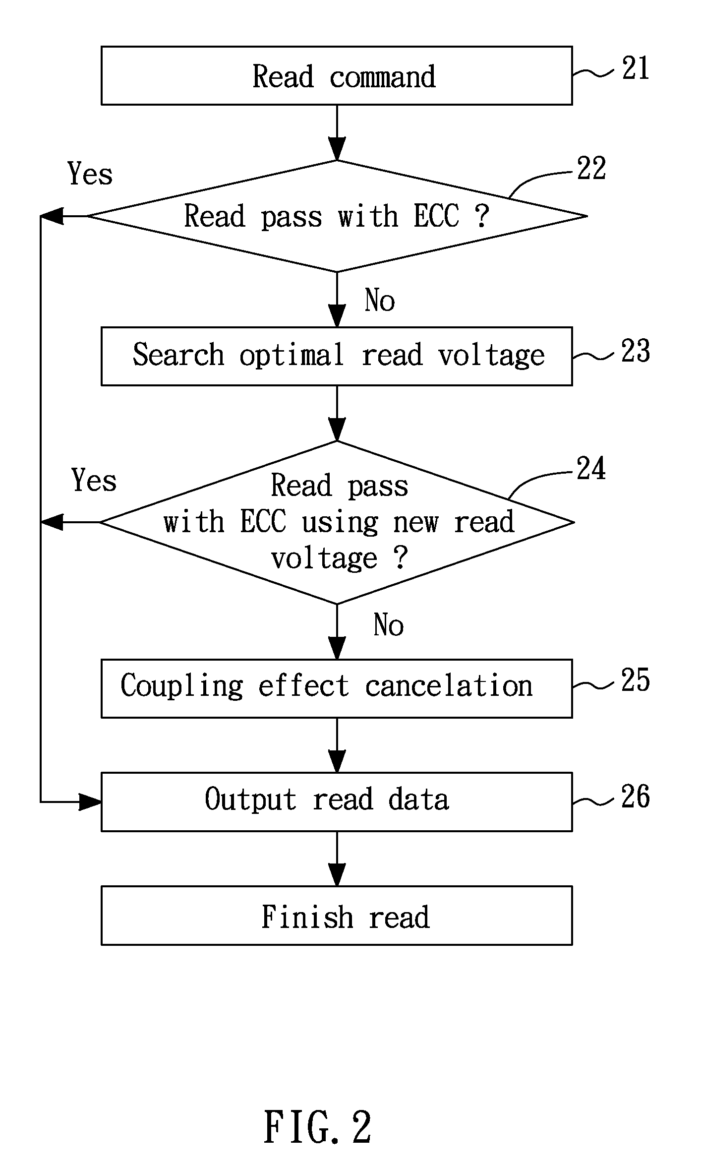
[0016]FIG. 2 is a flow diagram that illustrates a read flow of a flash memory according to one embodiment of the present invention. The embodiment may be adapted to a multi-level cell (MLC) flash memory as well as a single-level cell (SLC) flash memory.

[0017]Referring to FIG. 2, after the flash memory is requested by a read command (the step 21), the read data are checked for the compliance with error correction control (ECC) in the step 22. If the reading passes the ECC check, the read data are outputted (the step 26); otherwise, an optimal read voltage is searched in the step 23, followed by re-reading the flash memory using the newly searched read voltage to replace a default read voltage. This newly searched read voltage may be used to resolve the problem caused by distribution shift. The step 23 may be implemented by, but not limited to, methods disclosed, by the same assignee, in another U.S. patent application entitled “METHOD AND SYSTEM OF FINDING A READ VOLTAGE FOR A FLASH ...


PUM


Abstract

A method of reducing coupling effect in a flash memory is disclosed. A neighboring page is read, and a flag is set active if the neighboring page is an interfering page. Data are read from the neighboring page at least two more times using at least two distinct read voltages respectively. The threshold-voltage distributions associated with an original page and the neighboring page are transferred according to the read data and the flag.

Description

BACKGROUND OF THE INVENTION[0001]1. Field of the Invention[0002]The present invention generally relates to a flash memory, and more particularly to a method of reducing bit error rate for a flash memory.[0003]2. Description of the Prior Art[0004]Flash memory is a non-volatile solid state memory device that can be electrically erased and reprogrammed, and is a specific type of electrically erasable programmable read-only memory (EEPROM) device. Conventional flash memory stores a single bit of information in each memory cell such that each memory cell can be programmed to assume two possible states. The conventional flash memory is thus commonly referred to as single-level cell (SLC) flash memory or single-bit cell (SBC) flash memory. Modern flash memory is capable of storing two or more bits of information in each memory cell such that each memory cell can be programmed to assume more than two possible states. The modern flash memory is thus commonly referred to as multi-level cell (...

Claims


Application Information

Patent Timeline
Patent Type & Authority Applications(United States)
IPC IPC(8): G11C16/04G11C16/06
CPCG06F11/1048G11C16/3418G11C16/26G11C11/5642
Inventor CHOU, MING-HUNGHUANG, CHIEN-FUHUANG, HAN-LUNGCHO, SHIH-KENG
Owner JIANGSU HUACUN ELECTRONICS TECH CO LTD
Why Eureka
Try Eureka