Array substrate and manufacturing method and display device thereof

A technology of an array substrate and a manufacturing method, which is applied to the field of an array substrate and a manufacturing method thereof and a display device, can solve the problems of difference, influence on display effect, common electrode voltage change, etc., so as to avoid crosstalk phenomenon, eliminate coupling effect, and reduce resistance Effect

Inactive Publication Date: 2012-08-29
BEIJING BOE OPTOELECTRONCIS TECH CO LTD
View PDF6 Cites 28 Cited by
  • Summary
  • Abstract
  • Description
  • Claims
  • Application Information

AI Technical Summary

Problems solved by technology

[0006] The common electrode of the above-mentioned ADS product forms a whole, but due to the influence of large resistance, the coupling effect of the source-drain (SD) signal line to the common electrode cannot be resolved in time, resulting in the voltage change of the common electrode and the driving voltage in the pixel. Differences will produce differences, which will cause crosstalk phenomenon on the display screen and affect the display effect
The R-ADS technology that applies the above technical solutions also has the problem of crosstalk

Method used


Image

  • Array substrate and manufacturing method and display device thereof
  • Array substrate and manufacturing method and display device thereof
  • Array substrate and manufacturing method and display device thereof

Examples


Embodiment 1

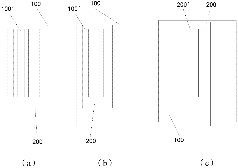
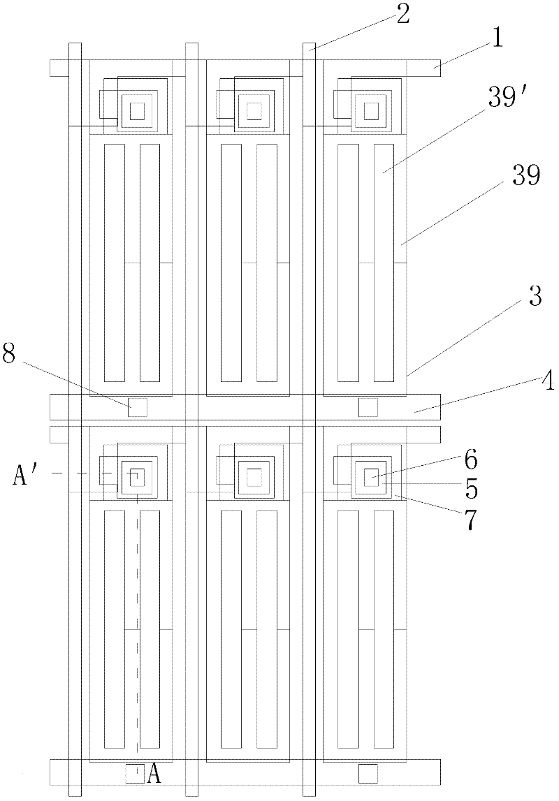
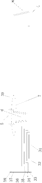
[0045] The ADS type array substrate of this embodiment, such as figure 2As shown, it includes: gate line 1, data line 2 and several thin film transistor pixel structures 3 between gate line 1 and data line 2 (each thin film transistor pixel structure corresponds to a pixel unit), each thin film transistor pixel structure 3 Including a thin film transistor and a display area, wherein the thin film transistor includes a gate, a gate insulating layer, an active layer, a source and a drain ( figure 2 not shown), the display area refers to the area used for display outside the thin film transistor (corresponding to the area where the pixel electrode is located), including the pixel electrode 39 and the common electrode ( figure 2 not shown), the common electrode is a block-shaped common electrode connected as a whole on the entire array substrate. The array substrate also includes at least one common electrode line 4 connected to the common electrode of the thin film transistor...

Embodiment 2

[0061] Since a number of common electrode lines 4 are added to the array substrate structure of Example 1, if the traditional ADS method is used, the common electrode lines 4 need to have a certain distance from the gate lines 1, which will cause them to block the normal light-emitting area and affect the aperture ratio. In order to increase the aperture ratio, the array substrate of this embodiment is arranged in such a way that TFTs face each other. Such as Figure 4 Shown (the cross-sectional view of each thin film transistor pixel structure and image 3 similar), among the several thin film transistor pixel structures 3 divided by the gate line 1, the thin film transistor regions of two adjacent rows of thin film transistor pixel structures 3 (that is, two adjacent rows of pixel units) are arranged adjacently, and the adjacent two rows of thin film transistor pixel structures The respective display areas of 3 are respectively arranged adjacent to the display areas of the ...

Embodiment 3

[0071] This embodiment provides a display device including the array substrate in Embodiment 1 or 2. The display device can be: liquid crystal panel, electronic paper, OLED panel, liquid crystal TV, liquid crystal display, digital photo frame, mobile phone, tablet computer, etc. Any product or part that has a display function.


PUM


Abstract

The invention discloses an array substrate, relating to the technical field of display. The array substrate comprises a plurality of grid lines and data lines formed on a substrate and a plurality of film transistor pixel structures formed between the grid lines and the data lines; each film transistor pixel structure comprises a film transistor and a display area; each display area is provided with a common electrode; and the array substrate further comprises at least one common electrode line which is connected with the common electrodes. The invention further discloses a manufacturing method and a display device of the array substrate. The array substrate provided by the invention prevents pictures from generating a crosstalk phenomenon.

Description

technical field [0001] The present invention relates to the field of display technology, in particular to an array substrate, a manufacturing method thereof, and a display device. Background technique [0002] Advanced Super Dimension Switch (ADS) is a planar electric field wide viewing angle core technology. Its core technical characteristics are: the electric field generated by the edge of the slit electrode in the same plane and the slit electrode layer and plate The electric field generated between the shape electrode layers forms a multi-dimensional electric field, so that all oriented liquid crystal molecules between the slit electrodes in the liquid crystal cell and directly above the electrodes can be rotated, thereby improving the working efficiency of the liquid crystal and increasing the light transmission efficiency. Advanced ultra-dimensional field conversion technology (ADS) can improve the picture quality of TFT-LCD products, with high resolution, high transmi...

Claims


Application Information

Patent Timeline
Patent Type & Authority Applications(China)
IPC IPC(8): H01L27/12H01L21/77G02F1/1362G02F1/1368G02F1/1343
CPCH01L27/124G02F1/136286
Inventor 姜文博董学陈东李成徐宇博陈小川薛海林陈希张弥李小和
Owner BEIJING BOE OPTOELECTRONCIS TECH CO LTD
Why Eureka
Try Eureka