Semiconductor Wafer-To-Wafer Bonding For Dissimilar Semiconductor Dies And/Or Wafers

a technology of semiconductor dies and/or wafers, which is applied in the direction of semiconductor devices, semiconductor/solid-state device details, electrical apparatus, etc., can solve the problems of low throughput of wafers, low efficiency of die-to-die bonding, and die-to-substrat bonding

Active Publication Date: 2011-03-03
QUALCOMM INC
View PDF12 Cites 48 Cited by
  • Summary
  • Abstract
  • Description
  • Claims
  • Application Information

AI Technical Summary

Problems solved by technology

These less efficient techniques includes die-to-die bonding, die-to-substrate bonding, and die-to

Method used


Image

  • Semiconductor Wafer-To-Wafer Bonding For Dissimilar Semiconductor Dies And/Or Wafers
  • Semiconductor Wafer-To-Wafer Bonding For Dissimilar Semiconductor Dies And/Or Wafers
  • Semiconductor Wafer-To-Wafer Bonding For Dissimilar Semiconductor Dies And/Or Wafers

Examples


Embodiment Construction

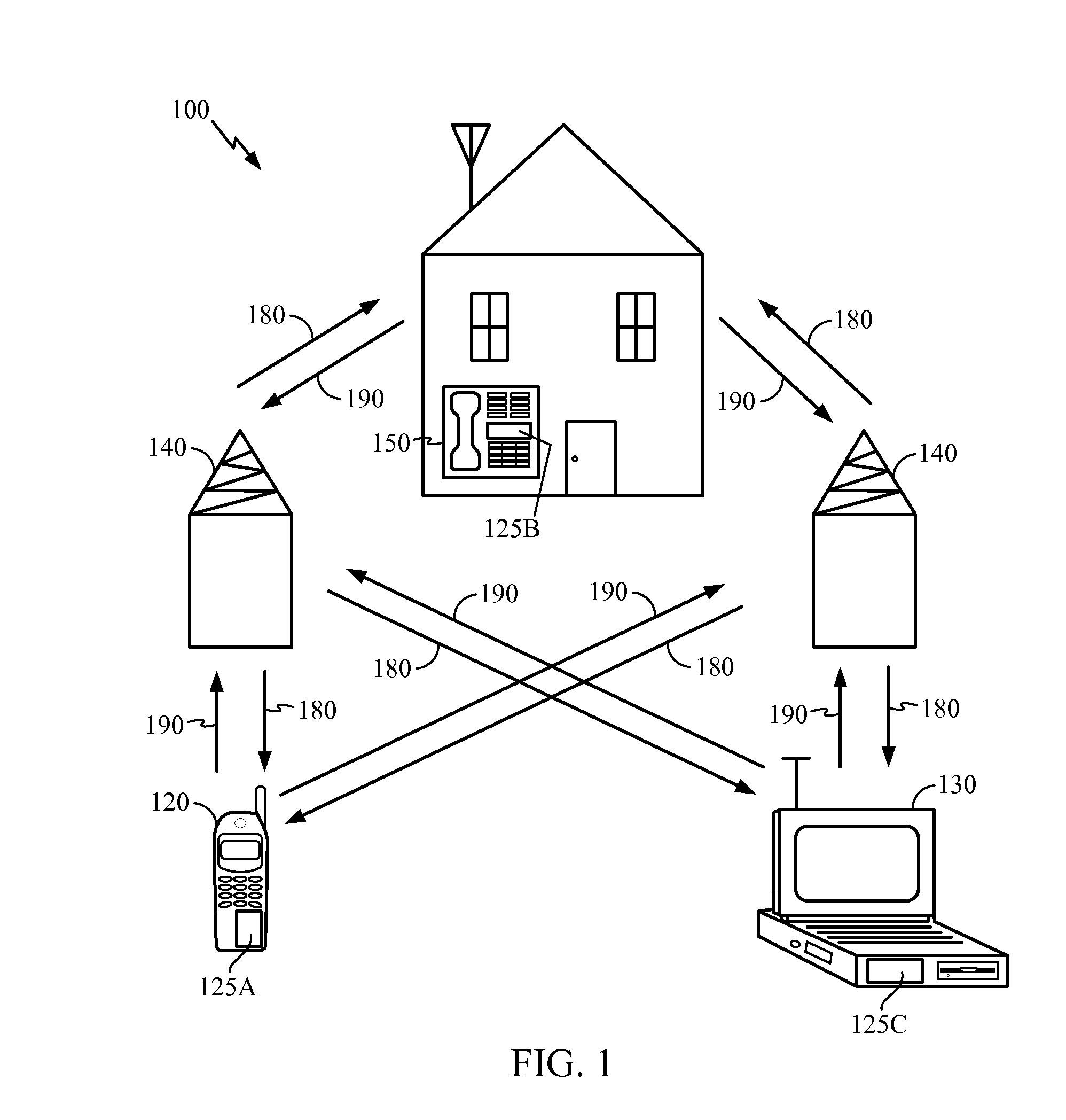
[0032]FIG. 1 is a block diagram showing an exemplary wireless communication system 100 in which an embodiment of the disclosure may be advantageously employed. For purposes of illustration, FIG. 1 shows three remote units 120, 130, and 150 and two base stations 140. It will be recognized that wireless communication systems may have many more remote units and base stations. Remote units 120, 130, and 150 include IC devices 125A, 125B and 125C, manufactured by the processes disclosed here. It will be recognized that any device containing an IC may also include semiconductor components having the disclosed features and / or components manufactured by the processes disclosed here, including the base stations, switching devices, and network equipment. FIG. 1 shows forward link signals 180 from the base station 140 to the remote units 120, 130, and 150 and reverse link signals 190 from the remote units 120, 130, and 150 to base stations 140.

[0033]In FIG. 1, the remote unit 120 is shown as a...


PUM


Abstract

A semiconductor manufacturing process for wafer-to-wafer stacking of a reconstituted wafer with a second wafer creates a stacked (3D) IC. The reconstituted wafer includes dies, die interconnects and mold compound. When stacked, the die interconnects of the reconstituted wafer correspond to die interconnects on the second wafer. Wafer-to-wafer stacking improves throughput of the manufacturing process. The reconstituted wafer may include dies of different sizes than those in the second wafer. Also, the dies of the reconstituted wafer may be singulated from a wafer having a different size than the second wafer. Thus, this wafer-to-wafer manufacturing process may combine dies and/or wafers of dissimilar sizes.

Description

TECHNICAL FIELD[0001]The present disclosure generally relates to integrated circuits (ICs). More specifically, the present disclosure relates to manufacturing stacked integrated circuits.BACKGROUND[0002]Semiconductor dies include collections of transistors and other components in a wafer. Commonly, these wafers are semiconductor materials, and, in particular, silicon. The semiconductor wafers are singulated or diced to form semiconductor dies.[0003]Semiconductor wafers may be stacked during manufacturing of products such as stacked ICs. Wafer-to-wafer bonding involves stacking the semiconductor wafers before being singulated into semiconductor dies. However, wafer-to-wafer bonding requires wafers and dies of equal size. Stacked ICs often include dies of different type or manufacturing process. For example, a stacked IC may have a memory device stacked on a processor. In this case, the memory device may not occupy as much die area as the processor.[0004]When the dies do not align for...

Claims


Application Information

Patent Timeline
IPC IPC(8): H01L27/06H01L21/60
CPCH01L2224/838H01L25/0657H01L2224/13099H01L2224/81193H01L2924/15311H01L24/16H01L2221/68377H01L2224/96H01L2225/06513H01L2924/14H01L2224/94H01L24/83H01L2924/01033H01L24/96H01L2924/18161H01L21/563H01L25/50H01L2221/68331H01L2924/01006H01L24/94H01L2224/81801H01L25/0655H01L24/81H01L2224/32145H01L2225/06541H01L2924/18165H01L2224/13025H01L2224/81H01L2924/181H01L2224/14181H01L2224/16145H01L24/97H01L2224/12105H01L2224/97H01L2924/18162H01L21/568H01L2224/04105H01L2224/1403H01L2224/14051H01L2224/16148H01L2224/73204H01L2924/00H01L2224/11H01L2224/83
Inventor CHANDRASEKARAN, ARVINDHENDERSON, BRIAN M.
Owner QUALCOMM INC
Why Eureka
Try Eureka