Three-dimensional multiprocessor system chip

A multi-processor system and processor technology, applied in the direction of electrical digital data processing, instruments, semiconductor devices, etc., can solve the problems of increased chip area consumption, intensified bus resource competition, complex network protocols, etc., to reduce signal delay time, The effect of shortening the length of the interconnection line and improving the product yield

Inactive Publication Date: 2008-03-19
SHANDONG UNIV
View PDF0 Cites 35 Cited by
  • Summary
  • Abstract
  • Description
  • Claims
  • Application Information

AI Technical Summary

Problems solved by technology

Three-dimensional integrated circuit manufacturing process, currently there is no commercial production capacity in the world
[0004] The data transmission method of the on-chip bus structure is to apply the method of computer system organization to the design of integrated circuit chips; the disadvantage of the on-chip bus structure is that when the number of on-chip processors increases, the competition for bus resources will intensify, resulting in data congestion.
The disadvantages of the Internet network structure are: the network protocol is more complicated, which increases the consumption of the chip area and increases the cost; at the same time, the serial data transmission method cannot give full play to the functional advantages of the system chip

Method used


Image

  • Three-dimensional multiprocessor system chip

Examples


Embodiment

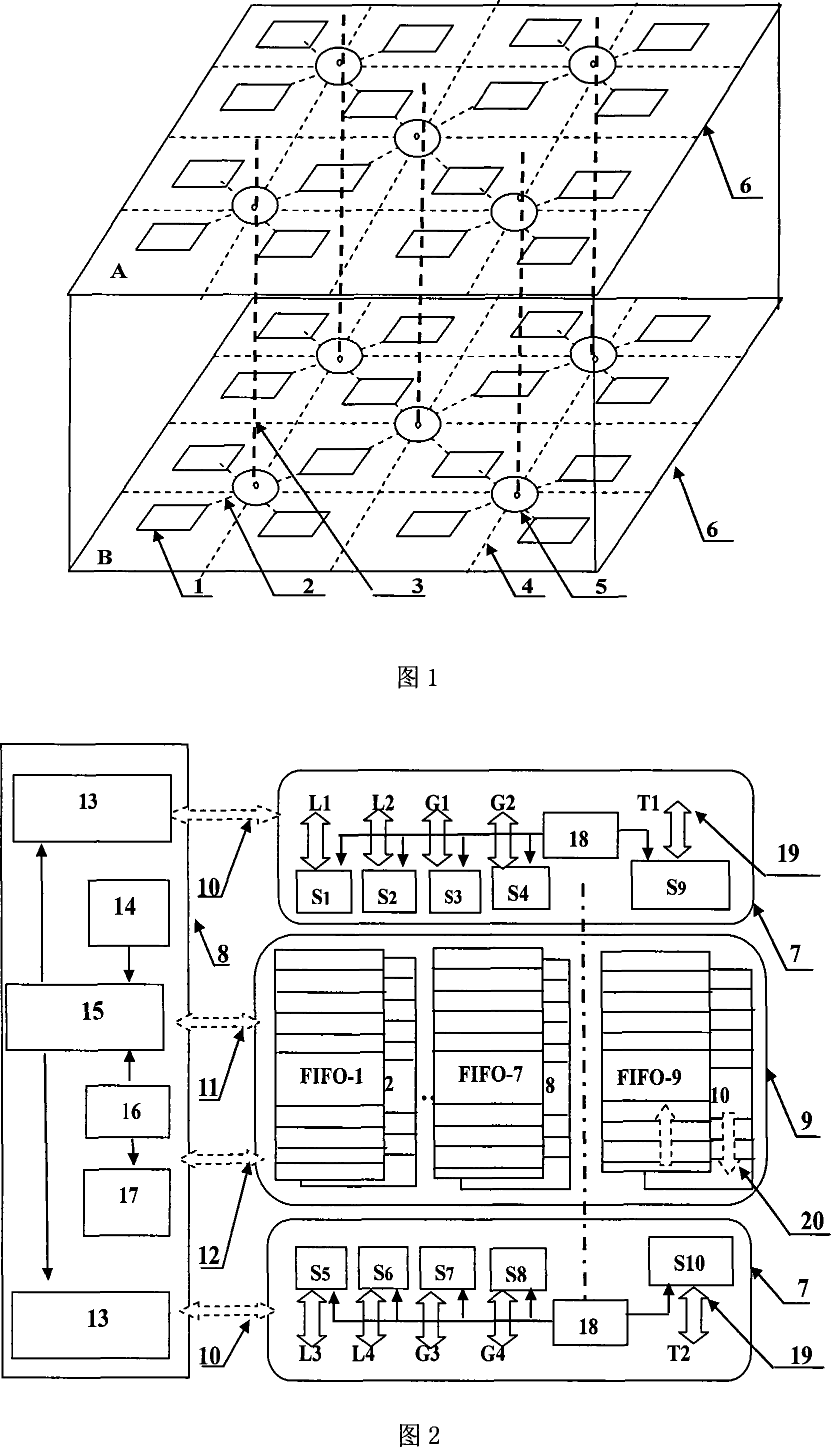
[0033] The embodiment of the present invention is shown in Figure 1-2, it is formed by stacking two VLSI chip wafers 6, 16 processor cores and 5 three-dimensional on-chip networks are integrated on the VLSI chip wafer 6 Router 5, the processors are connected through the three-dimensional network-on-chip router 5, the three-dimensional network-on-chip router 5 between each layer of wafers 6 is connected by a data channel in the vertical direction, and the three-dimensional network-on-chip router 5 is used to communicate between the 6 layers of wafers Parallel, bi-directional data transfer.

[0034]Described three-dimensional on-chip network router 5 is made up of first-in-first-out wave shift buffer memory (FIFO), synchronous matrix switch array, and digital routing decision-making module 8 and parallel network interface; Parallel network interface input port and synchronous matrix switch The arrays are connected; the output interface of the synchronous matrix switch array on o...


PUM


Abstract

The present invention relates to a chip of a three-dimensional multiprocessor system and belongs to the technical field of an integrate circuit design and manufacture. The present invention comprises a plurality of processor cores, a plurality of three-dimensional network routers on the chip and a wafer chip of a semiconductor integrate circuit that integrates a plurality of processor cores with a plurality of three-dimensional network routers on the chip. The present invention relates to a manufacturing method for utilizing wafer piles to assemble a three-dimensional integrate circuit and a transmitting method of parallel network data. The present invention has the advantages that: first, the part, whole or three-dimensional data transmissions are respectively accomplished by different channels, and the transmission congestion of the network data on the chip is relieved. Second, the three-dimensional chip structure reduces the chip area of a complicated SLSI (super-large-scale integration) and improves the product yield in the course of production. Third, the length of an interconnection line is shortened, the delay time of signals is reduced, and the system performance is enhanced.

Description

(1) Technical field [0001] The invention relates to a three-dimensional multiprocessor system chip, which belongs to the technical field of integrated circuit design and manufacture. (2) Background technology [0002] With the advancement of integrated circuit technology, tens of millions of gate circuits can be integrated on a single chip under the condition of deep submicron technology. Integrating multiple processors on one chip is the development direction of integrated circuits today and in the future. In 2007, both INTEL Corporation and AMD Corporation of the United States announced that they had produced a system chip with four processors. With the increase of the number of processors, the chip area is getting bigger and bigger, and the global wiring is getting longer and longer, so that in the deep submicron semiconductor process, the wiring delay between semiconductor devices is no longer negligible compared with the delay of the gate circuit. The deep submicron i...

Claims


Application Information

Patent Timeline
Patent Type & Authority Applications(China)
IPC IPC(8): G06F15/173G06F5/10H01L25/065H01L23/488H01L27/02
Inventor 曾凡太
Owner SHANDONG UNIV
Why Eureka
Try Eureka