
Method and device for evaluating electric performances of an fdsoi transistor

a technology of fdsoi transistor and electric performance, which is applied in the direction of electrical testing, electric digital data processing, instruments, etc., can solve the problems of relatively inaccurate, inconvenient use, and inability to accurately evaluate the electric performance of fdsoi transistors

Active Publication Date: 2011-03-03
COMMISSARIAT A LENERGIE ATOMIQUE ET AUX ENERGIES ALTERNATIVES
View PDF6 Cites 7 Cited by
  • Summary
  • Abstract
  • Description
  • Claims
  • Application Information

AI Technical Summary

Benefits of technology

[0011]Thus there is a need to propose a method for evaluating the electric performances of an FDSOI transistor allowing characterization of the defects present at an interface between a gate dielectric of the transistor and a semiconductor intended to form the channel of the transistor and at an interface between the semiconductor i

Problems solved by technology

But in this case, they are either not very accurate, or they require the use of adapted test structures.
This first method has the drawbacks of being relatively inaccurate and not allowing evaluation of defect densities of less than 1011 defects / cm2.
Although it is accurate, this method cannot be used on SOI transistors since it is not possible to measure a substrate current IB taking into account the buried dielectric present between the channel and the substrate composed of semiconductor.

Method used


Image

  • Method and device for evaluating electric performances of an fdsoi transistor
  • Method and device for evaluating electric performances of an fdsoi transistor
  • Method and device for evaluating electric performances of an fdsoi transistor

Examples


Embodiment Construction

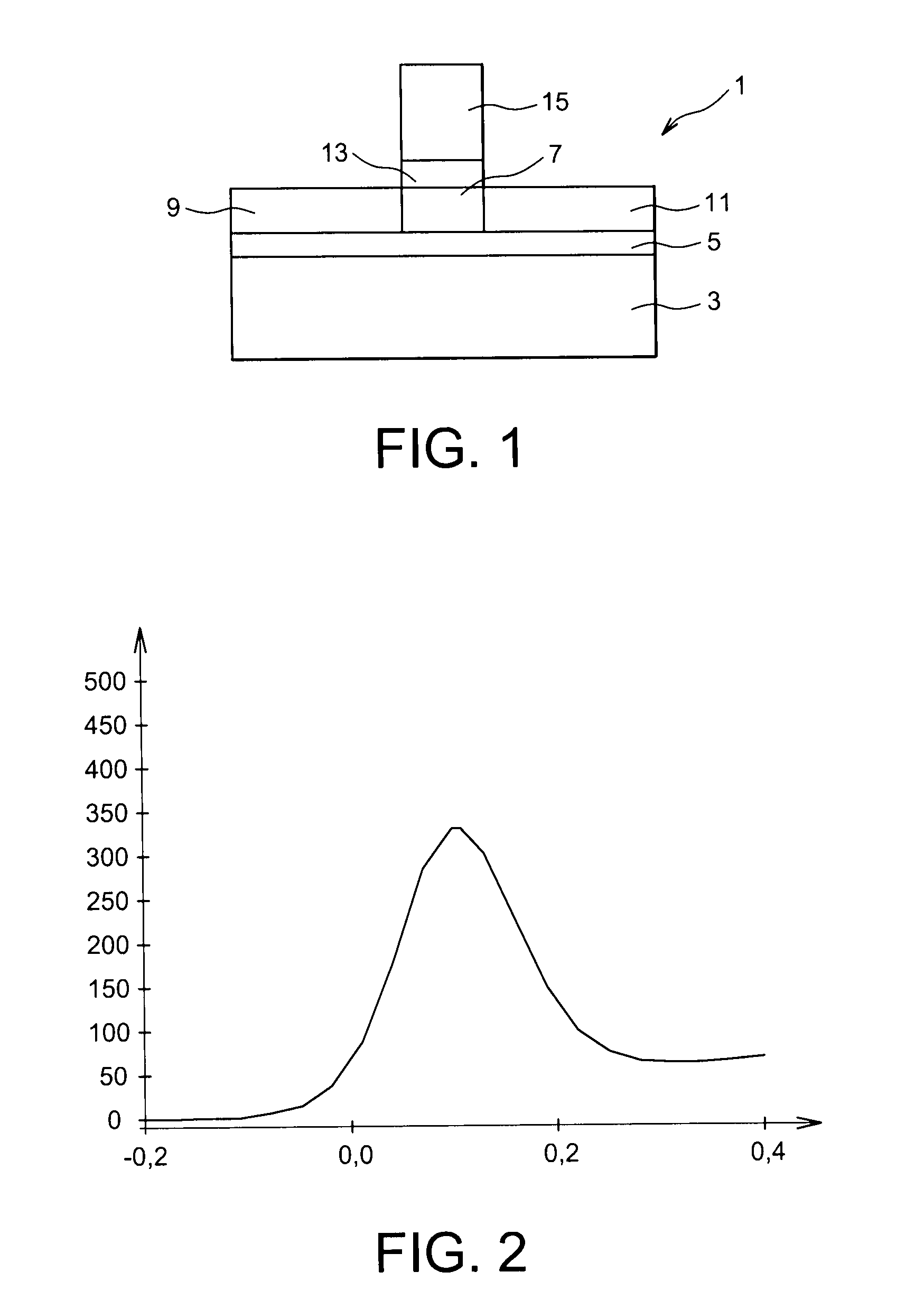
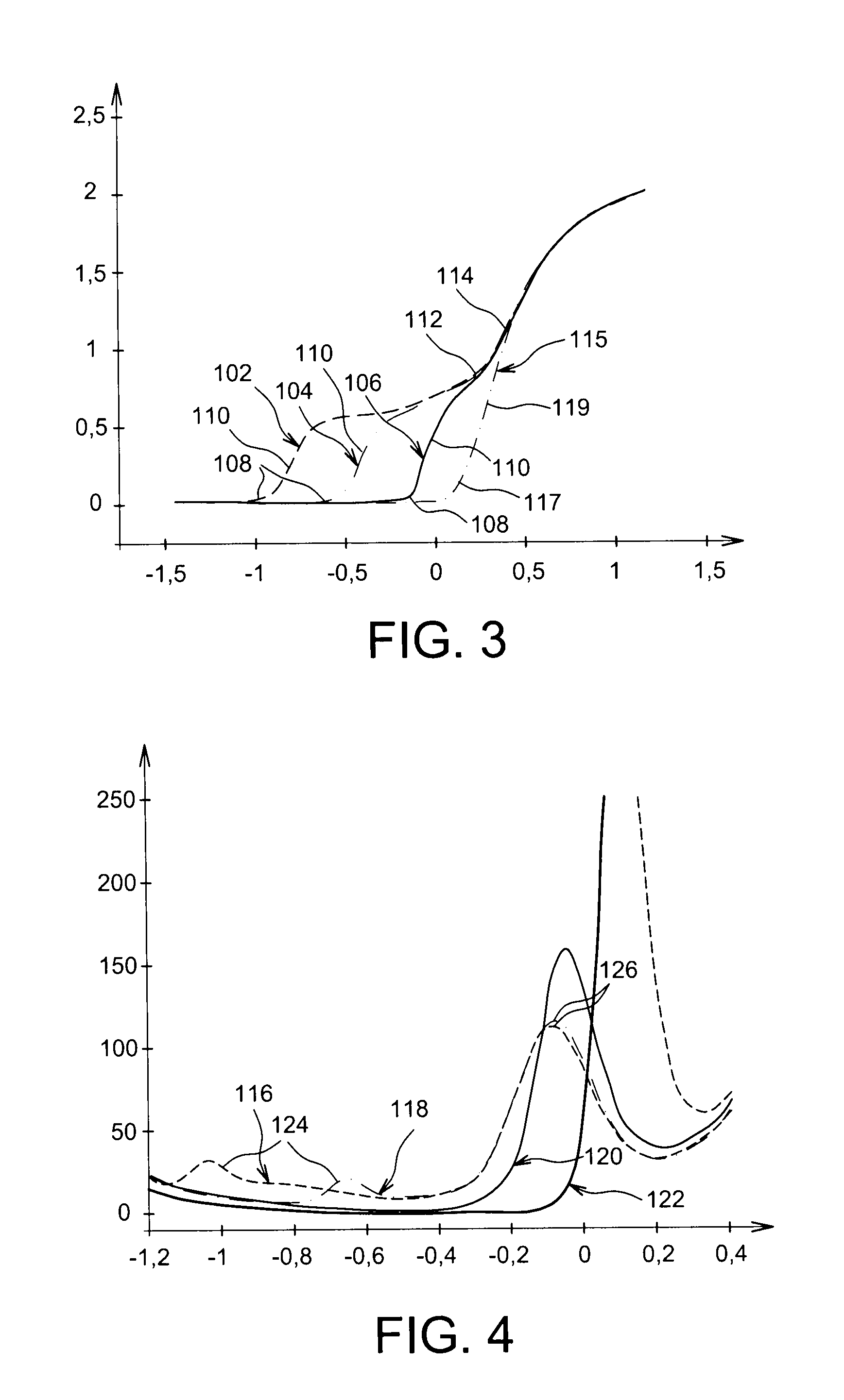
[0061]In the case of a MOS transistor of the bulk type, i.e. made on a bulk semiconducting substrate, it is possible to extract the density of the defects at the front interface, i.e. at the interface between the gate dielectric and the semiconducting portion forming the channel, by using the characteristics C(Vg) (capacitance of the transistor depending on the voltage Vg applied on the gate) and G(Vg) (conductance of the transistor depending on the voltage Vg applied on the gate). Indeed, by plotting the characteristic G(Vg), a low inversion regime peak appears, this peak being proportional to the density of defects at the front interface of the transistor. In the case of an FDSOI transistor, this peak also appears on the characteristic G(Vg) of this transistor. However, this peak is proportional to the accumulation of the defects at the front and rear interfaces because the characteristic G(Vg) is directly related to the electron density at the front and rear interfaces.

[0062]FIG....


PUM


Abstract

A method for evaluating the electric performances of an FDSOI transistor, including the steps of:measuring the capacitance and / or the conductance of the FDSOI transistor, by applying a rear voltage VBG>0 or VBG<0 on the substrate of the transistor, depending on a front voltage VFG applied on the gate of the transistor,calculating the theoretical values of the capacitance and / or the conductance of a transistor modeled by an electric circuit equivalent to the FDSOI transistor, for different selected theoretical values of defect densities Dit1, Dit2 at the dielectric-semiconductor interfaces of the modeled transistor,determining the real values of Dit1, Dit2 at the corresponding interfaces of the FDSOI transistor by a comparison between the measured values of the capacitance and / or the conductance of the FDSOI transistor and the calculated theoretical values of the capacitance and / or the conductance of the modeled transistor.

Description

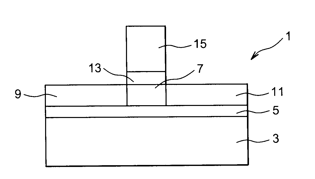
TECHNICAL FIELD[0001]The invention relates to a method and a device for evaluating the electric performances of FDSOI transistors, i.e. fully depleted transistors of the silicon-on-insulator type.[0002]The invention is notably used for electrically characterizing the semiconducting dielectric interfaces of FDSOI transistors by evaluating the defect densities at these interfaces, the electric performances of FDSOI transistors being directly dependent on the quality of these interfaces and therefore on the defect densities present at these interfaces.STATE OF THE PRIOR ART[0003]An example of an FDSOI transistor 1 is illustrated in FIG. 1. The transistor 1 is made on an SOI (silicon-on-insulator) type substrate including a substrate 3 composed of a semiconductor, for example silicon, on which is positioned a dielectric layer 5 for example composed of SiO2, forming a buried dielectric (BOX).[0004]A semiconducting layer, such as silicon, in which a channel region 7 and source 9 and drain...

Claims


Application Information

Patent Timeline
IPC IPC(8): G01R27/26
CPCG01R31/2642G01R31/2621
Inventor GARROS, XAVIERBRUNET, LAURENT
Owner COMMISSARIAT A LENERGIE ATOMIQUE ET AUX ENERGIES ALTERNATIVES
Learn More