Liquid crystal display device

a liquid crystal display and display device technology, applied in non-linear optics, instruments, optics, etc., can solve the problems of defective connection between the conductive paste and the conductivity applied surface, affecting affecting the stability of the electrical connection. , to achieve the effect of enhancing the mechanical strength of the liquid crystal display device, imparting conductivity, and stable electrical connection

Inactive Publication Date: 2011-03-03
PANASONIC LIQUID CRYSTAL DISPLAY CO LTD +1
View PDF4 Cites 5 Cited by
  • Summary
  • Abstract
  • Description
  • Claims
  • Application Information

AI Technical Summary

Benefits of technology

[0008]In the conventional liquid crystal display device, although a thickness of the glass substrate is approximately 0.2 mm to 0.5 mm, there may be a case where the thickness of the glass substrate is decreased to 0.05 mm or less for realizing the reduction of thickness, the reduction of weight, bending of a display screen of the liquid crystal display device or the like. In such a case, at the time of forming a transparent conductive film on the substrate SUB1 using an ITO vacuum sputtering method or a coating method of a conductive coating material or the like, there arises a drawback that the substrate SUB1 is easily broken.
[0010]The present invention has been made to overcome the above-mentioned drawbacks, and it is an object of the present invention to provide a liquid crystal display device which can improve mechanical strength of the liquid crystal display device and, at the same time, can ensure the electrical connection between lines formed on a second substrate (a substrate on which thin film transistors are formed, for example) and a first substrate (a substrate on which color filters are formed, for example).
[0026]According to the present invention, the substrate on which color filters are formed is formed using the resin substrate and hence, it is possible to enhance the mechanical strength of the liquid crystal display device. Further, by imparting the conductivity to the resin substrate and by establishing the electrical connection at the portion of the resin substrate which is exposed from the polarizer, it is possible to ensure the stable electrical connection between the lines formed on the second substrate (for example, the substrate on which the thin film transistors are formed) and the first substrate (for example, the substrate on which the color filters are formed).

Problems solved by technology

In such a case, at the time of forming a transparent conductive film on the substrate SUB1 using an ITO vacuum sputtering method or a coating method of a conductive coating material or the like, there arises a drawback that the substrate SUB1 is easily broken.
However, the polarization characteristic of the polarizer (polyvinyl alcoholic material) is generated by stretching the polarizer in a manufacturing step thereof and hence, the shrinkage of the polarizer is liable to occur with time.
Accordingly, even when electrical grounding is applied to the polarizer using the conductive paste or the like, there arises a drawback that the defective connection between the conductive paste and the conductivity applied surface is liable to occur due to the shrinkage of the polarizer.

Method used


Image

  • Liquid crystal display device
  • Liquid crystal display device
  • Liquid crystal display device

Examples


first embodiment

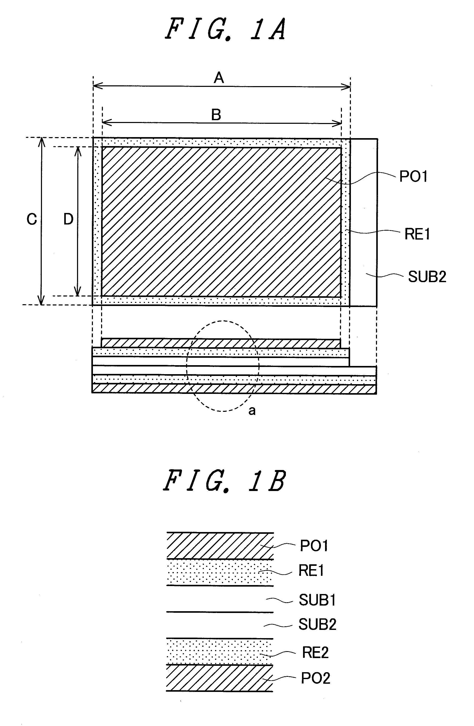
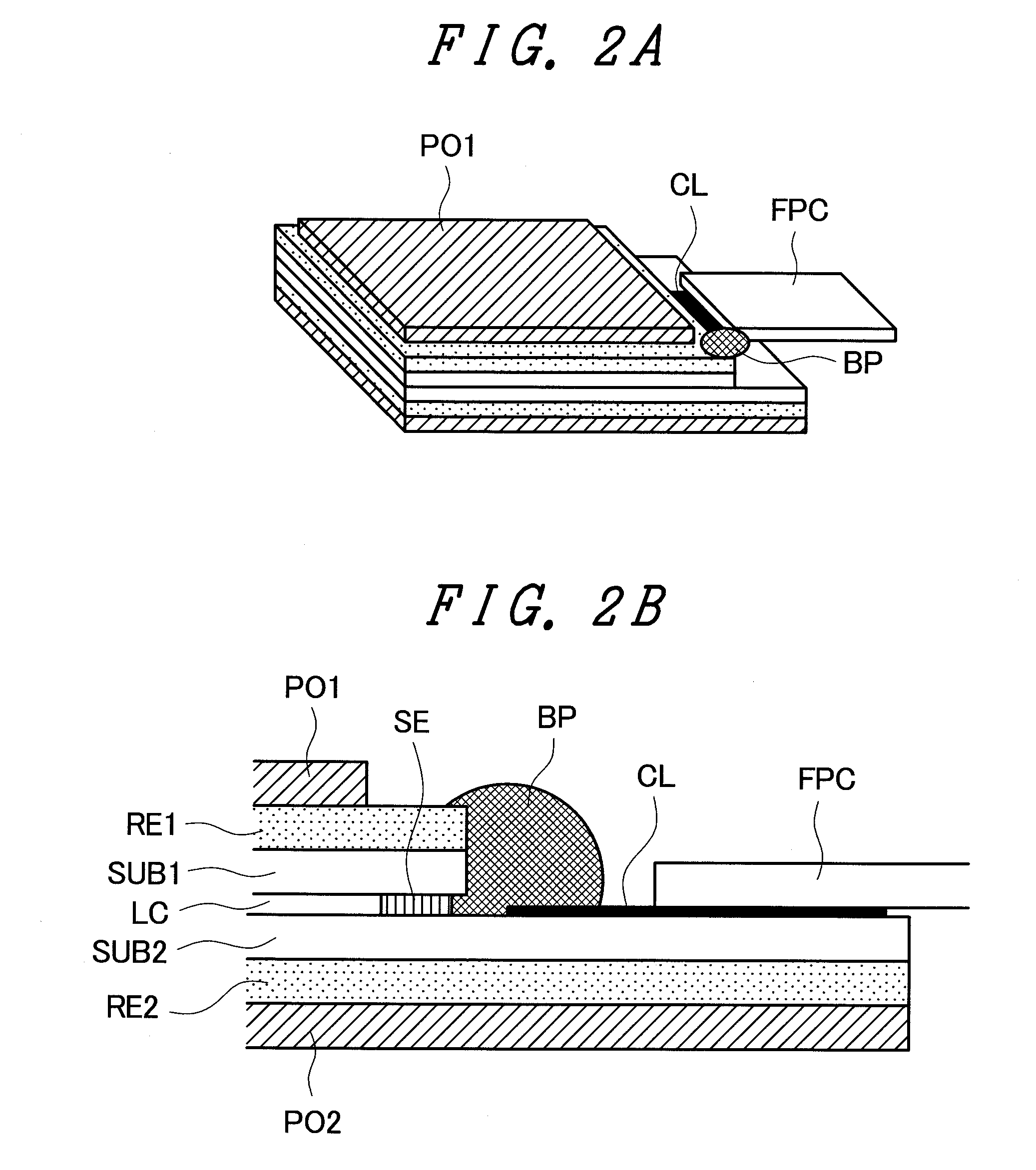
[0037]A liquid crystal display device according to the present invention is explained in detail hereinafter. FIG. 1A and FIG. 1B are views showing a liquid crystal display panel used in a liquid crystal display device of the present invention. Further, FIG. 2A and FIG. 2B show a mode in which the liquid crystal display panel shown in FIG. 1 and flexible printed circuit board lines (FPC lines) are connected to each other.

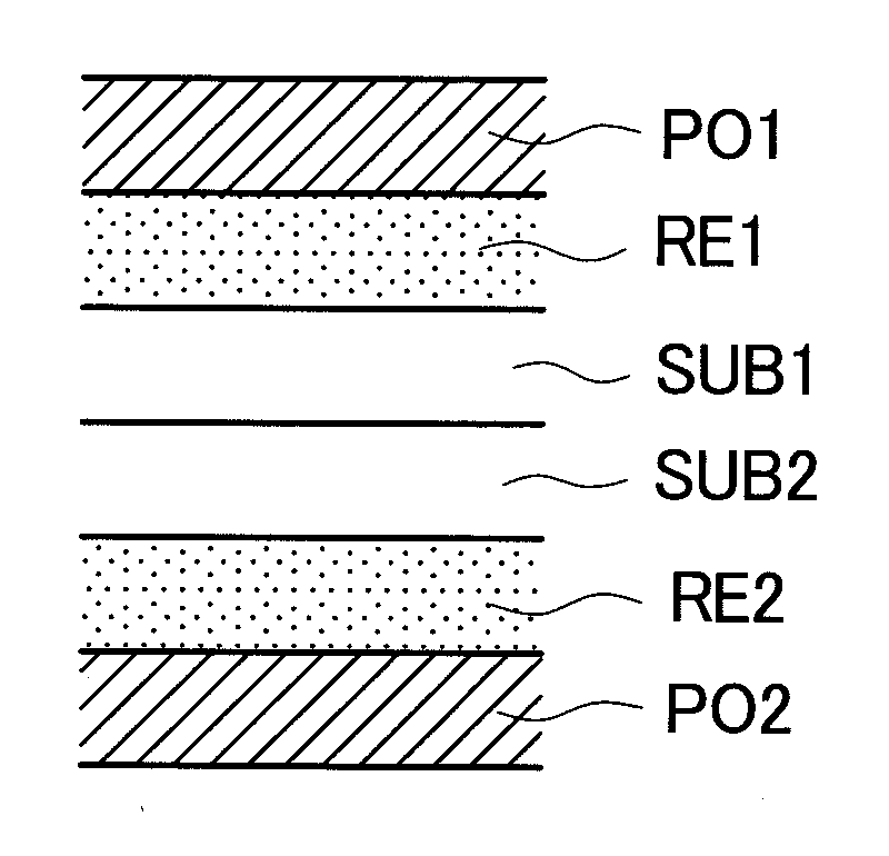
[0038]The liquid crystal display device of the present invention is characterized in that, in the liquid crystal display device where a substrate on which thin film transistors are formed and a substrate on which color filters are formed are arranged to face each other in an opposed manner, and a liquid crystal layer is arranged between both substrates, a resin substrate RE1 to which conductivity is imparted is formed on a substrate side on which the color filters are formed, a polarizer Pal is formed on an outer surface (surface opposite to a liquid crystal layer) o...

second embodiment

[0048]Further, in the second embodiment shown in FIG. 3A and FIG. 3B, a notched portion 1 is formed in a portion of the polarizer PO1 so as to expose a portion of the resin substrate RE1.

third embodiment

[0049]Further, in the third embodiment shown in FIG. 4A and FIG. 4B, a portion of the resin substrate RE1 is formed as a projection portion 2 which projects from the polarizer PO1 in a tab shape so as to expose the portion of the resin substrate RE1.

[0050]In all of first to third embodiments, the glass substrate (substrate SUB1) on which the color filters are formed and the glass substrate (substrate SUB2) on which the thin film transistors are formed are used as an example. However, the above-mentioned constitution may be adopted as a method for exposing a portion of a resin substrate from a polarizer also in the constitution of various substrates described later in the same manner.

[0051]FIG. 5A, FIG. 5B, FIG. 6A and FIG. 6B show a liquid crystal display device according to a fourth embodiment of the present invention. In the fourth embodiment, a resin substrate RE3 is used as a substrate on which color filters are formed. By directly forming the color filters on the resin substrat...


PUM

PropertyMeasurementUnit
thicknessaaaaaaaaaa
thicknessaaaaaaaaaa
thicknessaaaaaaaaaa

Abstract

In a liquid crystal display device including: a first substrate and a second substrate; and a liquid crystal layer which is arranged between the first substrate and the second substrate, the first substrate includes a resin substrate having conductivity and a polarizer, the polarizer is arranged on a surface of the resin substrate on a side opposite to a surface of the resin substrate which faces the second substrate in an opposed manner, a main surface of the resin substrate includes an exposure portion which exposes a portion of the main surface of the resin substrate from a main surface of the polarizer, a plurality of lines are formed on the second substrate, and the first substrate is electrically connected with at least one of the plurality of lines via the exposure portion.

Description

CROSS-REFERENCE TO RELATED APPLICATION[0001]The present application claims priority from Japanese application JP 2009-193938 filed on Aug. 25, 2009, the content of which is hereby incorporated by reference into this application.BACKGROUND OF THE INVENTION[0002]The present invention relates to a liquid crystal display device, and more particularly to a liquid crystal display device which can improve mechanical strength of the liquid crystal display device where a first substrate (for example, a substrate on which color filters are formed) and a second substrate (for example, a substrate on which thin film transistors are formed) are arranged to face each other in an opposed manner and a liquid crystal layer is arranged between both substrates, and can ensure the stable electrical connection between lines formed on the substrate on which the thin film transistors are formed and the substrate on which the color filters are formed.[0003]The liquid crystal display device has been popular...

Claims


Application Information

Patent Timeline
Patent Type & Authority Applications(United States)
IPC IPC(8): G02F1/1333
CPCG02F1/1333G02F2202/22G02F2202/16G02F1/1345
Inventor SASAKI, SUSUMUTAKAHASHI, KATSUYUUNAGATA, TETSUYAAZUMA, HITOSHIYAGUCHI, TOMIONAKANO, YASUSHI
Owner PANASONIC LIQUID CRYSTAL DISPLAY CO LTD
Why Eureka
Try Eureka