Semiconductor memory device capable of suppressing peak current
a memory device and semiconductor technology, applied in the field of semiconductor memory devices, can solve the problems of high write voltage, low write speed, and miswrite, and achieve the effect of reducing the number of devices
- Summary
- Abstract
- Description
- Claims
- Application Information
AI Technical Summary
Benefits of technology
Problems solved by technology
Method used
Image


Examples
first embodiment
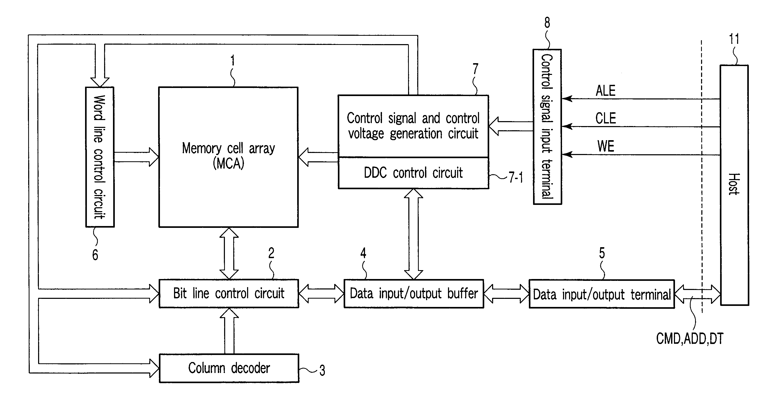
[0038]FIG. 2 shows the schematic configuration of a NAND flash memory for storing eight-valued data of three bits.
[0039]A memory cell array 1 includes a plurality of bit lines, a plurality of word lines, and common source lines, and in which electrically rewritable memory cells constituted of, for example, EEPROM cells are arranged in a matrix form. A bit line control circuit 2 for controlling bit lines, and a word line control circuit 6 are connected to the memory cell array 1.
[0040]In the bit line control circuit 2, by reading data of a memory cell in the memory cell array 1 through a bit line, by detecting a state of the memory cell in the memory cell array 1 through the bit line, or by applying a write control voltage to the memory cell in the memory cell array 1 through the bit line, data is written to the memory cell. A column decoder 3, and a data input / output buffer 4 are connected to the bit line control circuit 2. A data storage circuit included in the bit line control cir...
PUM
 Abstract
Description
Claims
Application Information