
Semiconductor package and method of manufacturing the semiconductor package

a semiconductor and semiconductor chip technology, applied in the direction of semiconductor devices, semiconductor/solid-state device details, electrical apparatus, etc., can solve the problems of frequent contact failure between adjacent bonding wires or between the bonding wire and the semiconductor chips, and achieve the effect of miniaturizing the semiconductor package, reducing the loop height of the bonding wire, and improving the reliability of the semiconductor packag

Active Publication Date: 2011-03-24
SAMSUNG ELECTRONICS CO LTD
View PDF4 Cites 16 Cited by
  • Summary
  • Abstract
  • Description
  • Claims
  • Application Information

AI Technical Summary

Benefits of technology

[0010]Example embodiments provide a semiconductor package capable of providing a free wiring routing design.
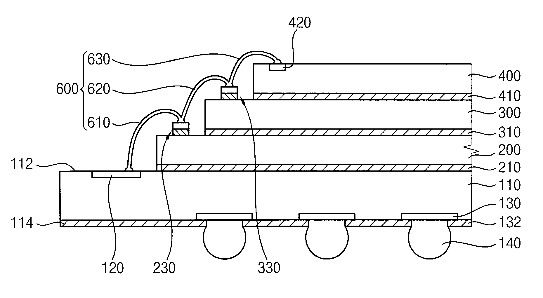
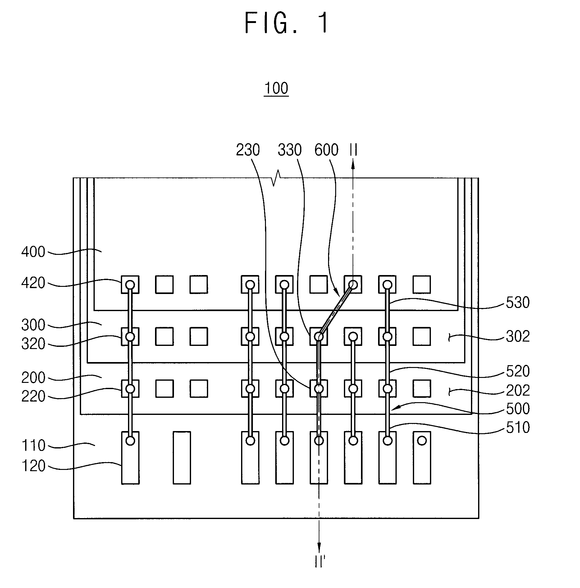
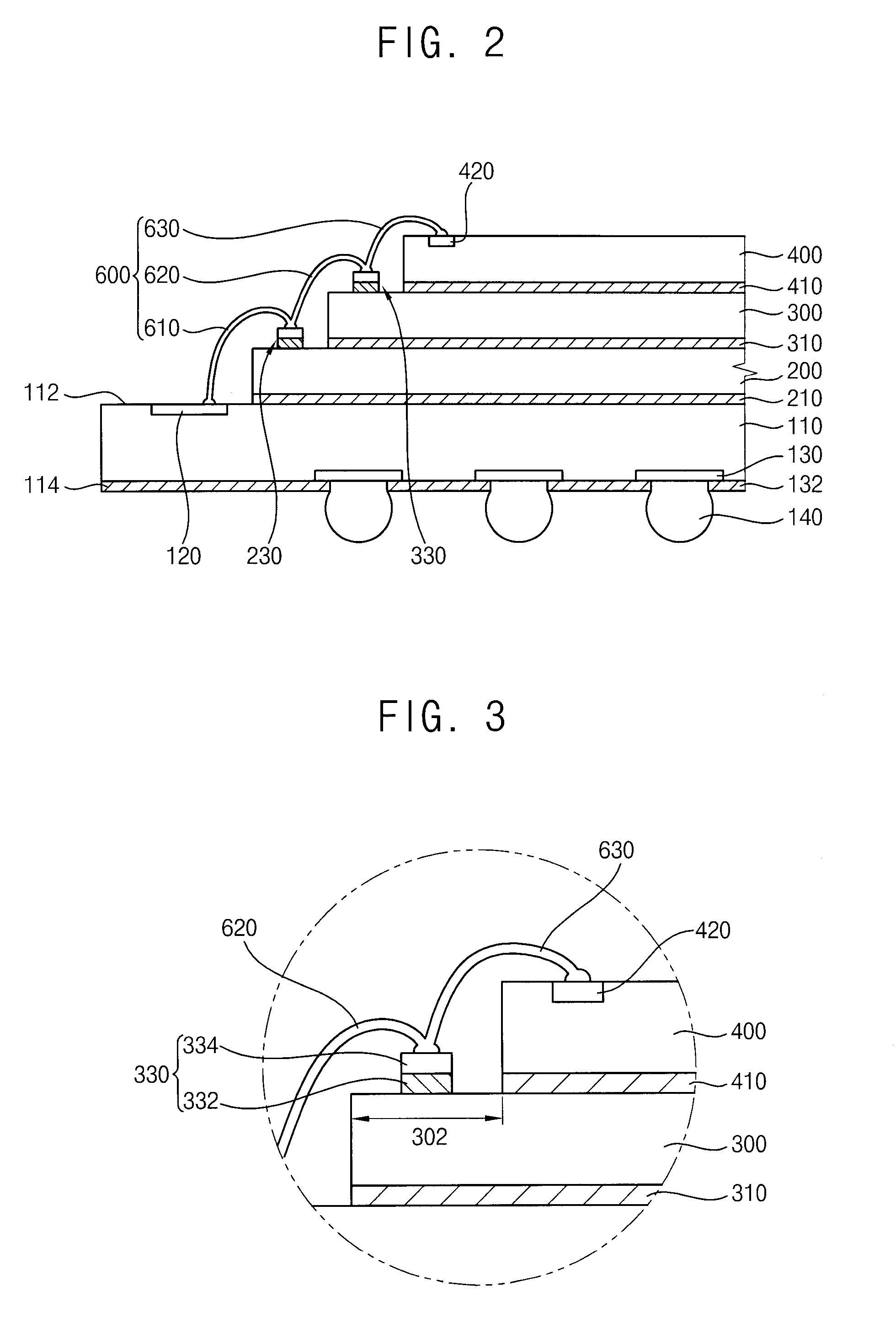
[0031]Accordingly, the stepped pads may provide a free wiring route design for a bonding wire. Additionally, the stepped pads may compensate for the height differences between the stacked semiconductor chips to decrease the loop height of the bonding wire to thereby miniaturize the semiconductor package. Further, the bonding wire may be prevented from making contact with the adjacent another bonding wire that is spaced apart by a relatively small distance or the semiconductor chips, to thereby improve reliability of the semiconductor package.

Problems solved by technology

Especially, because the length and loop height of the bonding wire for electrically connecting a chip pad of the uppermost semiconductor chip to a bonding pad of the mounting substrate are increased, contact failures between adjacent bonding wires or between the bonding wire and the semiconductor chips occur frequently.

Method used


Image

  • Semiconductor package and method of manufacturing the semiconductor package
  • Semiconductor package and method of manufacturing the semiconductor package
  • Semiconductor package and method of manufacturing the semiconductor package

Examples


Embodiment Construction

[0041]Various example embodiments will be described more fully hereinafter with reference to the accompanying drawings, in which example embodiments are shown. Example embodiments may, however, be embodied in many different forms and should not be construed as limited to example embodiments set forth herein. Rather, these example embodiments are provided so that this disclosure will be thorough and complete, and will fully convey the scope of example embodiments to those skilled in the art. In the drawings, the sizes and relative sizes of layers and regions may be exaggerated for clarity.

[0042]It will be understood that when an element or layer is referred to as being “on,”“connected to” or “coupled to” another element or layer, it can be directly on, connected or coupled to the other element or layer or intervening elements or layers may be present. In contrast, when an element is referred to as being “directly on,”“directly connected to” or “directly coupled to” another element or...


PUM


Abstract

A semiconductor package includes a first semiconductor chip, a second semiconductor chip, a stepped pad, a plurality of first bonding wires and a second bonding wire. The first semiconductor chip is stacked on a substrate having a plurality of bonding pads, the first semiconductor chip having a plurality of first chips pads formed along a side portion of the first semiconductor chip. The second semiconductor chip is stacked like a step of a staircase on the first semiconductor chip to form a stepped portion through which the first chip pads are exposed on the first semiconductor chip, the second semiconductor chip having a plurality of second chip pads formed along a side portion of the first semiconductor chip. The stepped pad is arranged between the first chip pads on the stepped portion of the first semiconductor chip, the stepped pad including an adhesive pad adhered to the first semiconductor chip and a conductive pad formed on the adhesive pad. A plurality of the first bonding wires electrically connect between the one second chip pad and the one first chip pad and / or between the one first chip pad and the one bonding pad. The second bonding wire electrically connects between the one second chip pad and the one bonding pad using the stepped pad.

Description

PRIORITY STATEMENT[0001]This application claims priority under 35 U.S.C. §119 to Korean Patent Application No. 2009-90340, filed on Sep. 24, 2009 in the Korean Intellectual Property Office (KIPO), the entire contents of which are herein incorporated by reference.BACKGROUND[0002]1. Field[0003]Example embodiments relate to a semiconductor package and a method of manufacturing the semiconductor package. More particularly, example embodiments relate to a semiconductor package including semiconductor chips that are stacked on a substrate and electrically connected to the substrate by a plurality of bonding wires and a method of manufacturing the semiconductor package.[0004]2. Description of the Related Art[0005]Generally, semiconductor devices are manufactured by a fabrication (“fab”) process for forming electrical circuits including electrical elements on a semiconductor substrate, e.g., a silicon wafer, an electrical die sorting (EDS) process for inspecting electrical properties of chi...

Claims


Application Information

Patent Timeline
IPC IPC(8): H01L25/065H01L21/60H01L23/52
CPCH01L23/49575H01L2924/07802H01L24/48H01L24/49H01L24/78H01L24/85H01L25/0657H01L25/50H01L2224/0401H01L2224/04042H01L2224/05624H01L2224/05639H01L2224/05644H01L2224/05647H01L2224/48091H01L2224/4813H01L2224/48145H01L2224/48227H01L2224/48247H01L2224/48463H01L2224/4911H01L2224/49171H01L2224/49175H01L2224/73265H01L2224/78301H01L2224/85H01L2225/06506H01L2225/0651H01L2924/01013H01L2924/01014H01L2924/01029H01L2924/01047H01L2924/01079H01L2924/01082H01L2924/014H01L2924/15311H01L2224/32145H01L2224/32225H01L2224/32245H01L2924/01006H01L2924/01023H01L2924/01033H01L2224/92247H01L2924/10253H01L2225/06562H01L2224/48147H01L2224/05554H01L24/05H01L2924/00014H01L2924/00H01L2924/00012H01L24/73H01L2924/181H01L2224/85181H01L2224/45099H01L23/48
Inventor KOOK, JOONG-KYO
Owner SAMSUNG ELECTRONICS CO LTD
Learn More