Window type BGA semiconductor package and its substrate

a semiconductor package and window-type technology, applied in semiconductor devices, semiconductor/solid-state device details, printed circuits, etc., can solve problems such as electrical shorts

Inactive Publication Date: 2010-06-08
POWERTECH TECHNOLOGY INC
View PDF1 Cites 3 Cited by
  • Summary
  • Abstract
  • Description
  • Claims
  • Application Information

AI Technical Summary

Benefits of technology

[0005]The main purpose of the present invention is to provide a window-type BGA semiconductor package and its substrate to avoid electrical short between the plating line stubs and the bonding wires with no relationship of corresponding connections leading to electrical failure of the semiconductor package.
[0006]The second purpose of the present invention is to provide a window-type BGA semiconductor package and its substrate for reducing the loop heights of the bonding wires and to avoid electrical short between the bonding wires and the plating line stubs by oblique and various designs of plating line stubs.
[0007]The third purpose of the present invention is to provide a window-type BGA semiconductor package and its substrate to decrease circuit layers of a substrate to reduce costs.

Problems solved by technology

However, there are still some plating line stubs remained on the substrate connected to the bonding fingers leading to possible electrical short caused by bonding wires.

Method used


Image

  • Window type BGA semiconductor package and its substrate
  • Window type BGA semiconductor package and its substrate
  • Window type BGA semiconductor package and its substrate

Examples


Embodiment Construction

[0016]Please refer to the attached drawings, the present invention will be described by means of embodiment below.

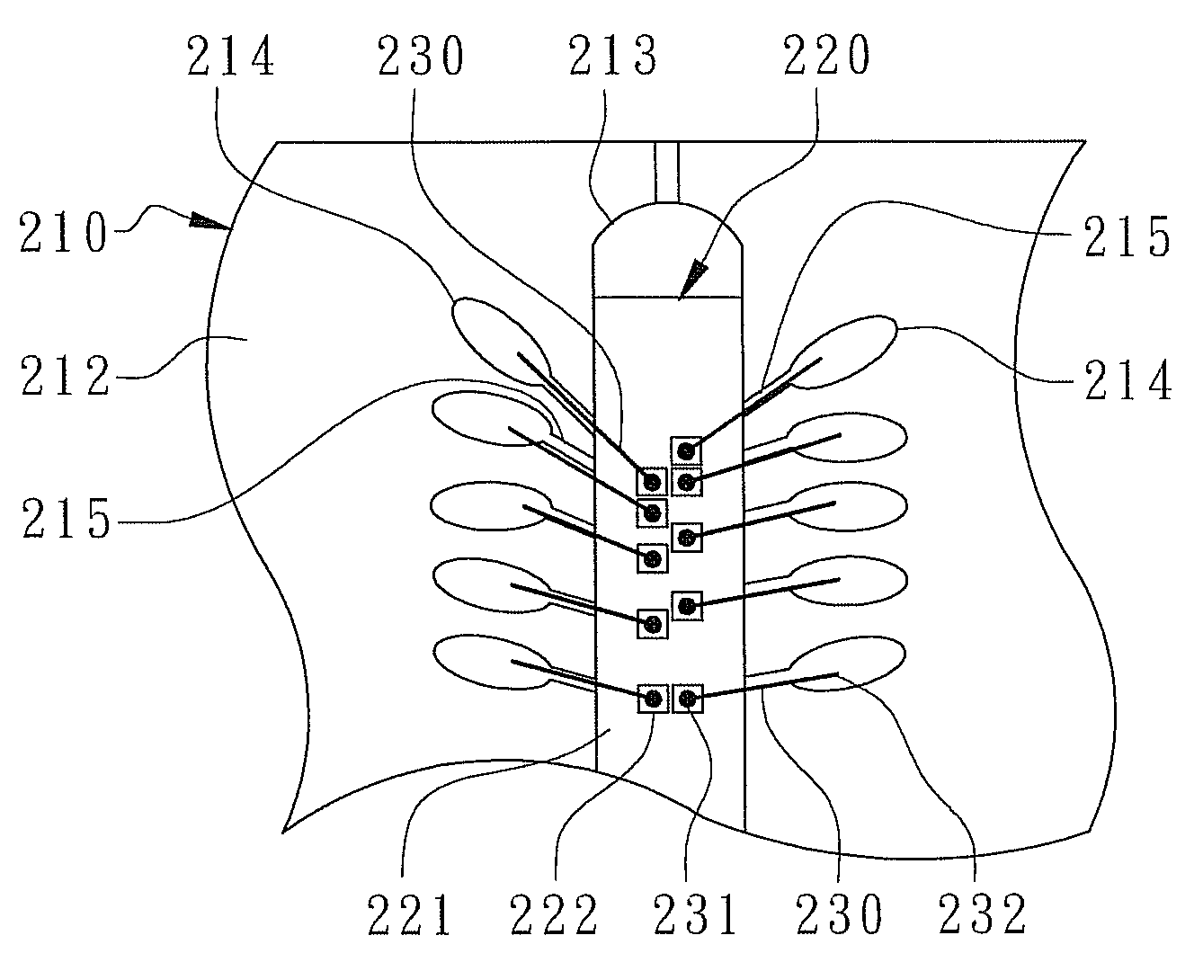
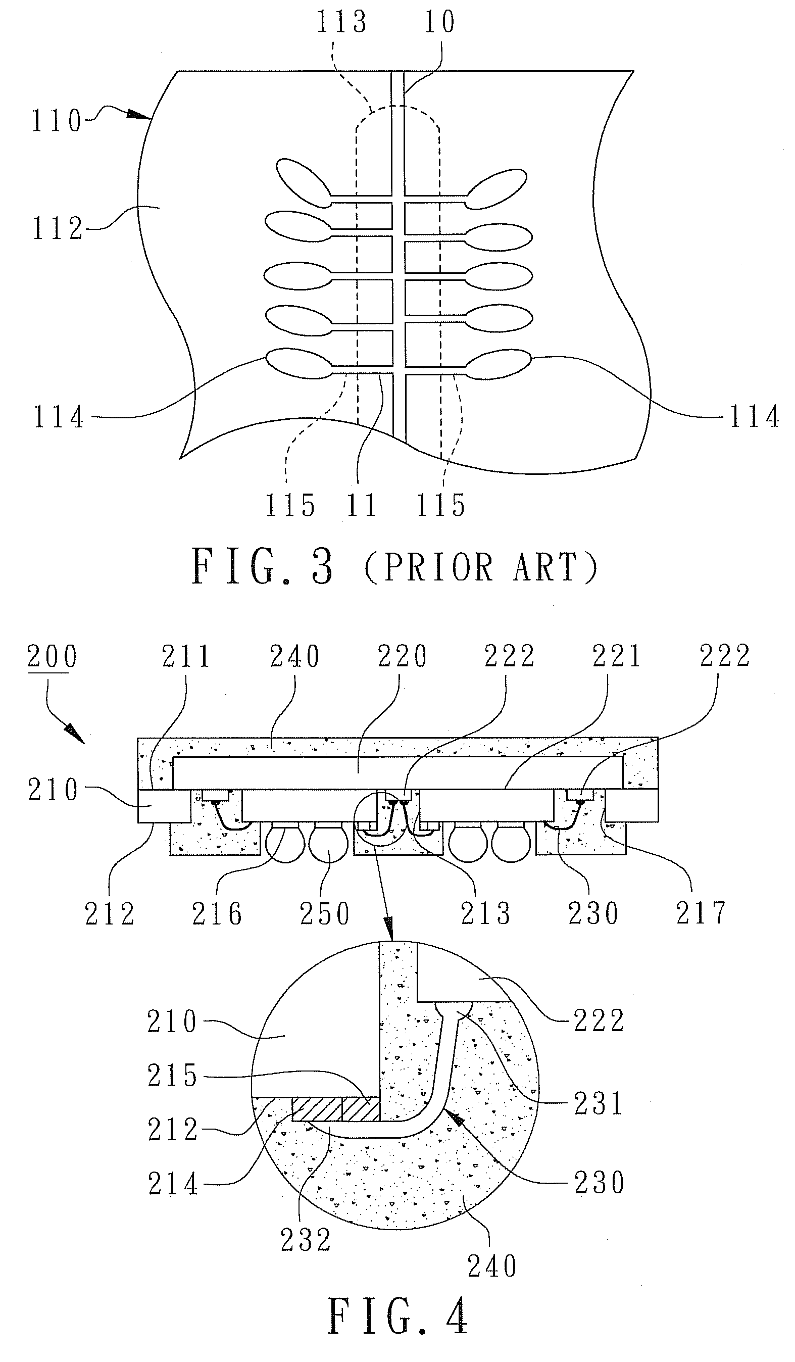
[0017]As shown in FIG. 4, a window-type BGA semiconductor package 200 primarily comprises a substrate 210, a chip 220, and a plurality of bonding wires 230. The substrate 210 has a top surface 211, a bottom surface 212, and a wire-bonding slot 213 for passing the bonding wires 230. The top surface 211 of the substrate 210 is used for attaching the chip 220. The wire-bonding slot 213 is a long and narrow through hole located at the center area of the substrate 210 penetrating the substrate 210 from the top surface 211 to the bottom surface 212. Generally speaking, the substrate 210 is served as a chip carrier with single-layer or multiple-layer circuits such as single-layer or multiple-layer printed circuit boards.

[0018]As shown in FIG. 5 and FIG. 6, the substrate 210 includes a plurality of bonding fingers 214 and a plurality of plating line stubs 215. The bonding finger...


PUM


Abstract

A window-type BGA semiconductor package is revealed, primarily comprising a substrate with a wire-bonding slot, a chip disposed on a top surface of the substrate, and a plurality of bonding wires passing through the wire-bonding slot. A plurality of plating line stubs are formed on a bottom surface of the substrate, connect the bonding fingers on the substrate and extend to the wire-bonding slot. The bonding wires electrically connect the bonding pads of the chip to the corresponding bonding fingers of the substrate. The plating line stubs are compliant to the wire-bonding paths of the bonding wires correspondingly connected at the bonding fingers, such as parallel to the overlapped arrangement, to avoid electrical short between the plating line stubs and the bonding wires with no corresponding relationship of electrical connections.

Description

FIELD OF THE INVENTION[0001]The present invention relates to semiconductor devices, especially to a window-type BGA (Ball Grid Array) semiconductor package and its substrate.BACKGROUND OF THE INVENTION[0002]Window-type BGA semiconductor package is a very common semiconductor package using a substrate with a wire-bonding slot as a chip carrier. Normally, a semiconductor chip is disposed on the top surface of the substrate and a plurality of external terminals such as solder balls are disposed on the bottom surface of the substrate. Moreover, a plurality of bonding wires pass through the wire-bonding slot to electrically connect the chip and the substrate. The substrate has a plurality of bonding fingers disposed on the bottom surface thereof for wire-bonding connection. In order to enhance bondability of the bonding fingers, it is necessary to form a plating layer on bonding fingers. During substrate manufacturing processes, before forming the wire-bonding slot, a plating bus line is...

Claims


Application Information

Patent Timeline
Patent Type & Authority Patents(United States)
IPC IPC(8): H01L23/48H01L23/52H01L29/40
CPCH01L23/13H01L23/49838H01L24/49H01L2924/014H01L2924/01033H05K3/242H01L2924/15311H01L2924/01082H01L2924/01079H01L2924/01078H01L2924/01028H01L2224/49171H01L2224/48465H01L2224/4824H01L2224/48091H01L24/48H01L2924/00014H01L2924/00H01L2924/181H01L2224/05554H01L2224/45099H01L2224/05599H01L2924/00012
Inventor FAN, WEN-JENGLIU, YI-LINGHUANG, SHIN-HUIYU, TSAI-CHUAN
Owner POWERTECH TECHNOLOGY INC
Why Eureka
Try Eureka