Negative-resistance device with the use of magneto-resistive effect

a negative resistance and magnetoresistive technology, applied in the field of negative resistance devices with the use of magnetoresistive effects, can solve the problems that the negative resistance devices having a different voltage region cannot be prepared by the same materials, and the amplifying apparatus cannot obtain a stable gain, so as to achieve the effect of superior linearity

Active Publication Date: 2011-09-06
CANON ANELVA CORP
View PDF4 Cites 11 Cited by
  • Summary
  • Abstract
  • Description
  • Claims
  • Application Information

AI Technical Summary

Benefits of technology

[0016]Furthermore, the negative-resistance device may be configured so that the means for applying the magnetic field is formed of a permanent magnetic layer, and the negative-resistance device further comprises an insulation layer to avoid electrical short between the permanent magnetic layer and the magneto-resistive device, the first electrode layer and the second electrode layer.
[0020]In the present invention, a negative resistance is developed based on a mechanism that the negative resistance is generated based on a change of balance state in magnetization by moderating a bias voltage, and consequently, the present invention can provide a negative-resistance device having a negative-resistance region with superior linearity to that of a conventional negative-resistance device. The present invention is also directed for devices to have various current / voltage characteristics to be prepared by using the same materials, and to realize the negative-resistance device which can be flexibly applied to various electronics fields.

Problems solved by technology

Such existence of a non-linear region causes a problem that when the diode is applied to an amplifying apparatus, the amplifying apparatus cannot obtain a stable gain.
Accordingly, the voltage region developing the negative resistance is determined by the material, so that a negative-resistance device having a different voltage region cannot be prepared by the same materials.

Method used


Image

  • Negative-resistance device with the use of magneto-resistive effect
  • Negative-resistance device with the use of magneto-resistive effect
  • Negative-resistance device with the use of magneto-resistive effect

Examples


embodiment 1

[0080]As is described above, in order to obtain a stable negative resistance in the present invention, it is necessary to provide the magnetization direction of the magnetic free layer of a magneto-resistive device which is used in a negative-resistance device so as to be stable only in a state of being parallel to the magnetization direction of a magnetic pinned layer.

[0081]An example of the negative-resistance device satisfying such a condition is illustrated in FIG. 8. A negative-resistance device 80 in FIG. 8 includes a magneto-resistive device 89 including a magnetic pinned layer 81, an intermediate layer 82 and a magnetic free layer 83, and electrode layers 84 and 85 for applying voltage to the magneto-resistive device 89. The electrode layers 84 and 85 are formed from a metal such as copper and gold having high electric conductivity. The negative-resistance device 80 is further provided with means for applying the external magnetic field to the magneto-resistive device 89 in ...

embodiment 2

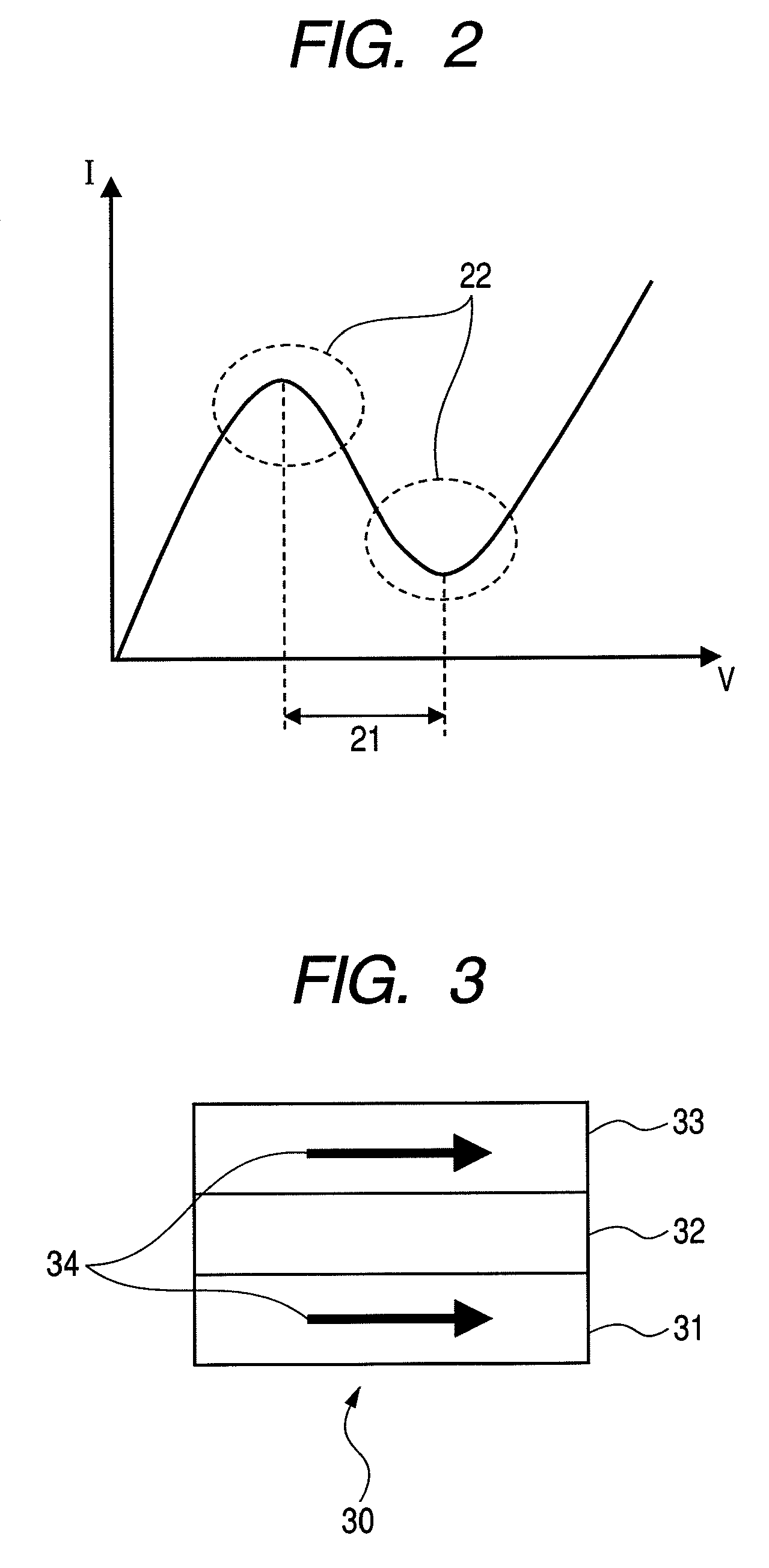
[0085]In the above described Embodiment 1, the negative-resistance device is configured so as to cause continuous magnetization reversal by realizing a stable condition in the device only when the magnetization directions of the magnetic free layer and the magnetic pinned layer are parallel through applying the external magnetic field to the magneto-resistive device, and by controlling or modulating the magnetization reversal of the magnetic free layer. However, the magnetization reversal can be also controlled by using a shift of the hysteresis region in characteristics of change of resistance with respect to external magnetic field instead of applying the external magnetic field.

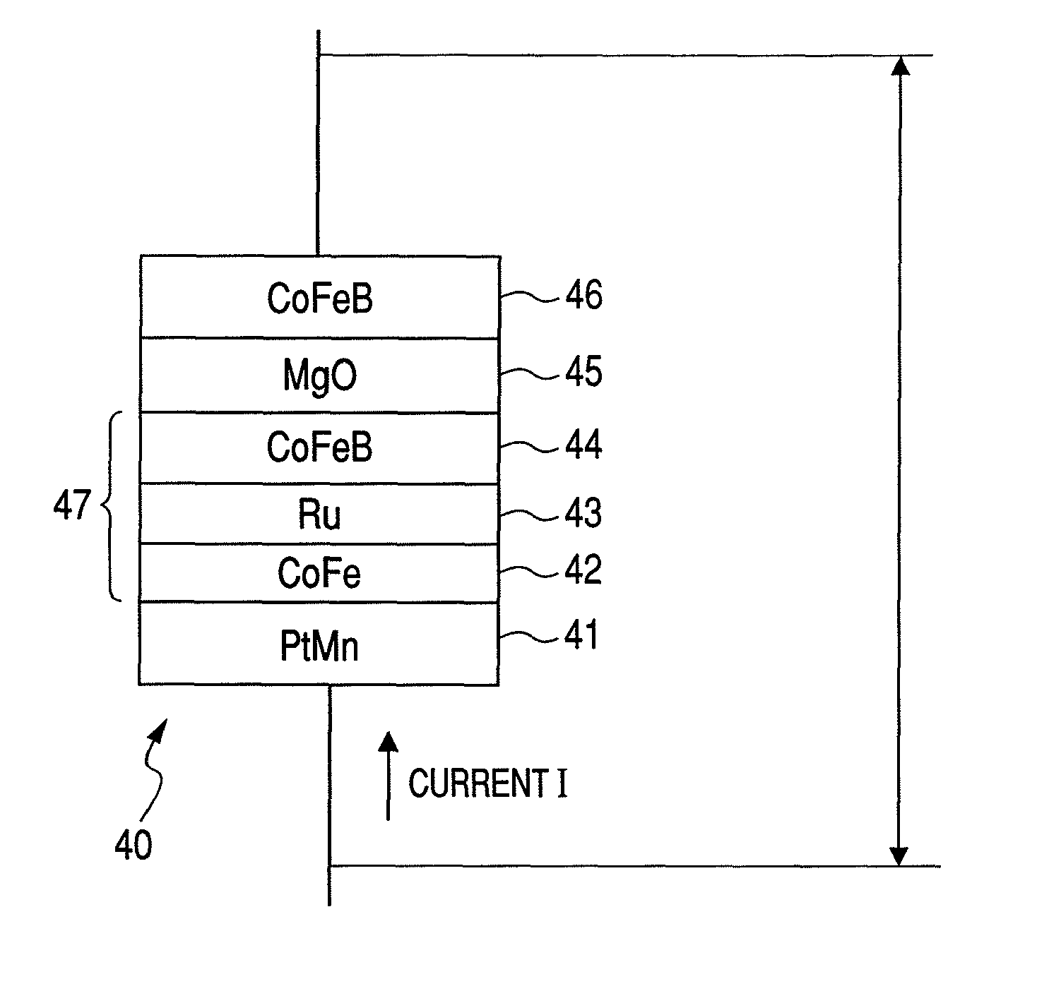
[0086]The example will now be described with reference to the spin valve type of a magneto-resistive device 40 illustrated in FIG. 4. A hysteresis region 51 illustrated in FIG. 5 is shifted to right and left on the graph by changing the film thickness of an intermediate layer 45 of a magneto-resistive devi...

embodiment 3

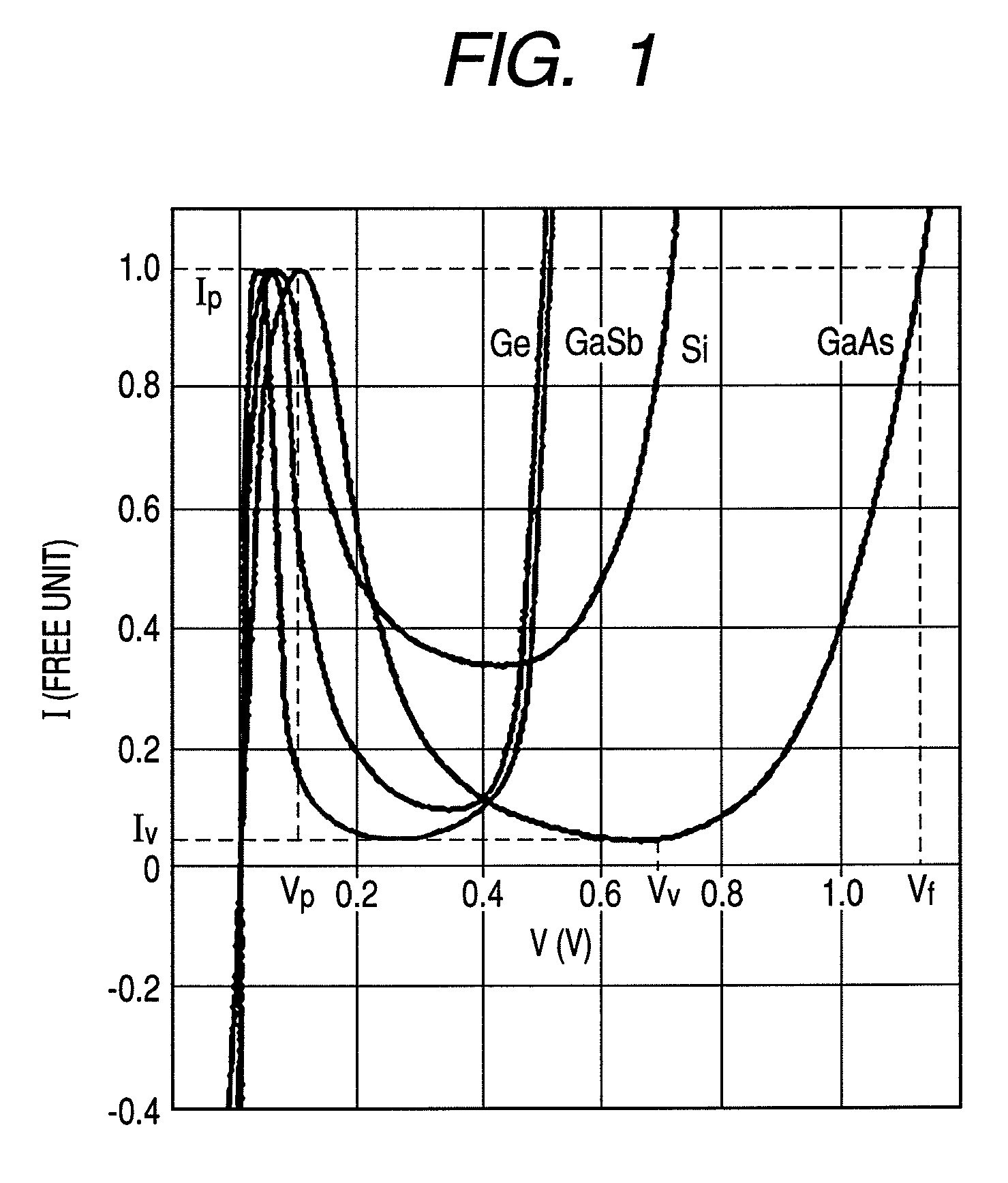
[0095]When RP is defined as an electric resistance of a magneto-resistive device in which the magnetization direction of the magnetic free layer is parallel to that of the magnetic pinned layer, and RAP is defined as an electric resistance of a magneto-resistive device in which the magnetization direction is anti-parallel, a magnetoresistance ratio (MR ratio) of the magneto-resistive device is defined as (RAP−RP) / RP. A peak valley ratio in current / voltage characteristics is determined by the magnitude of the magnetoresistance ratio. Therefore, the peak valley ratio can be increased by using a magneto-resistive device showing a large magnetoresistance ratio, and accordingly the negative-resistance device can be obtained which is suitable for application to an oscillator, an amplifier, a mixer, a switching device and the like. On the other hand, a magneto-resistive device showing a small magnetoresistance ratio may not cause sufficient negative-resistance characteristics, even though ...


PUM


Abstract

A magneto-resistive device has a magnetic free layer (33), a magnetic pinned layer (31) having a magnetic moment larger than that of the magnetic free layer, and an intermediate layer (32) provided between the magnetic free layer and the magnetic pinned layer. The negative-resistance device is characterized in that the negative-resistance device shows negative resistance by making the magnetic free layer continually change the magnetization direction along with the increase of the voltage which is applied to a magneto-resistive device so that electrons flow into the negative-resistance device from a magnetic free layer side.

Description

CROSS-REFERENCES TO RELATED APPLICATIONS[0001]This application is a continuation application of International Application No. PCT / JP2007 / 069019, filed on Sep. 28, 2007, the entire contents of which are incorporated by reference herein.TECHNICAL FIELD[0002]The present invention relates to a negative-resistance device with the use of a magneto-resistive effect.BACKGROUND ART[0003]A tunnel diode represented by an Esaki diode is known as a conventional negative-resistance device (for instance, in Patent Document 1). The negative resistance shown by the tunnel diode originates in a tunnel phenomenon, and in the case of the Esaki diode, for instance, the negative resistance is realized by enhancing impurity concentrations of P type and N type in a PN junction diode.[0004]FIG. 1 illustrates current / voltage characteristics of an Esaki diode which has been prepared from various materials (Ge, GaSb, Si and GaAs). FIG. 2 schematically illustrates these characteristics. Reference numeral 21 in ...

Claims


Application Information

Patent Timeline
Patent Type & Authority Patents(United States)
IPC IPC(8): H01L29/82G11C11/02
CPCB82Y25/00G11C11/14H01F10/3254H01F10/3272H01L29/885H01L43/08H10N50/10
Inventor MAEHARA, HIROKIKUBOTA, HITOSHIFUKUSHIMA, AKIOYUASA, SHINJISUZUKI, YOSHISHIGENAGAMINE, YOSHINORI
Owner CANON ANELVA CORP
Why Eureka
Try Eureka