Fingerprint sensing device with interposer structure

a technology of fingerprint and interposer, which is applied in the field of fingerprint sensing devices, can solve problems such as unsatisfactory aesthetic effects, and achieve the effects of improving capacitive coupling, improving capacitive coupling, and improving capacitive coupling

Active Publication Date: 2016-12-08
FINGERPRINT CARDS ANACATUM IP AB
View PDF7 Cites 6 Cited by
  • Summary
  • Abstract
  • Description
  • Claims
  • Application Information

AI Technical Summary

Benefits of technology

[0023]In one embodiment of the invention, in the case where one interposer structure is located on each of said sensing elements, the interposer structures may be formed in a material having a dielectric constant higher than a dielectric constant of the adhesive. An improved capacitive coupling between a finger and a sensing element can be achieved by providing an interposer structure having a dielectric constant which is higher than the surrounding adhesive. Thereby, the electric field between a finger placed on the sensing surface and the sensing element can b focused towards the respective sensing elements by means of the difference in dielectric constant. Accordingly, a further improved fingerprint sensing device can be provided.
[0024]According to one embodiment of the invention, the plurality of interposer structures may be arranged in alignment with boundaries between the sensing elements, such that a central portion of each sensing element is not covered by an interposer structure. For the above configuration of interposer elements, where at least a central portion of the sensing element is not covered by the interposer structure, the interposer structures may be formed in a material having a dielectric constant lower than a dielectric constant of the adhesive in order to achieve the above described effect of improved capacitive coupling between the sensing element and a finger. The adhesive will then fill the space between interposer structures such that an inhomogeneous layer is formed with respect to the dielectric constant of the materials, and where the higher dielectric constant of the adhesive provides the improved capacitive coupling.
[0025]According to one embodiment of the invention, the interposer structures may be arranged on the sensing chip at locations outside of a sensing area of the sensing chip, the sensing area being defined by the array of sensing elements. Thus, the interposer can be arranged to form a frame partially surrounding the array of sensing elements. The adhesive can then be arranged primarily within the frame formed by the interposer elements
[0026]According to one embodiment of the invention, the plurality of interposer structures may comprise a photoresist. By using a photoresist, the interposer structures can be formed using conventional photolithography and development processes, which simplifies the overall process flow. Moreover, a photoresist can easily be tailored to have a specific dielectric constant so that a desired ratio of dielectric constants can be achieved.
[0027]According to one embodiment of the invention, the sensing device may further comprise a bond wire arranged between a bond pad on the sensing chip and a substrate on which the sensing chip is arranged, wherein a bond loop height of the bond wire is lower than the interposer structure. It may also be possible to have a bond wire loop height which is slightly higher than the height of the interposer structure, in which case the protective plate may push down on the bond wire when the protective plate is attached to the sensing chip.
[0028]In one embodiment of the invention, the sensing device may further comprise a via connection through said sensing chip to electrically connect the sensing chip to a substrate. A via connection, commonly referred to as a through-silicon via (TSV) connection, can be used to electrically connect the sensing chip to readout circuitry on a substrate without using wire bonding. TSV connection is for example used when wire bonding is undesirable or unpractical, such as when the desired height of the interposer structures is lower than a height of the wire bond. This situation could for example occur when the sensor shall be utilized with a very thick protective plate such as e.g. a cover glass in a mobile phone.

Problems solved by technology

However, a direct electrical contact between the finger and the pixel may cause problems related to electrostatic discharge (ESD).
Moreover, the metallic portions of the surface may oxidize, resulting in undesirable aesthetic effects.

Method used


Image

  • Fingerprint sensing device with interposer structure
  • Fingerprint sensing device with interposer structure
  • Fingerprint sensing device with interposer structure

Examples


Embodiment Construction

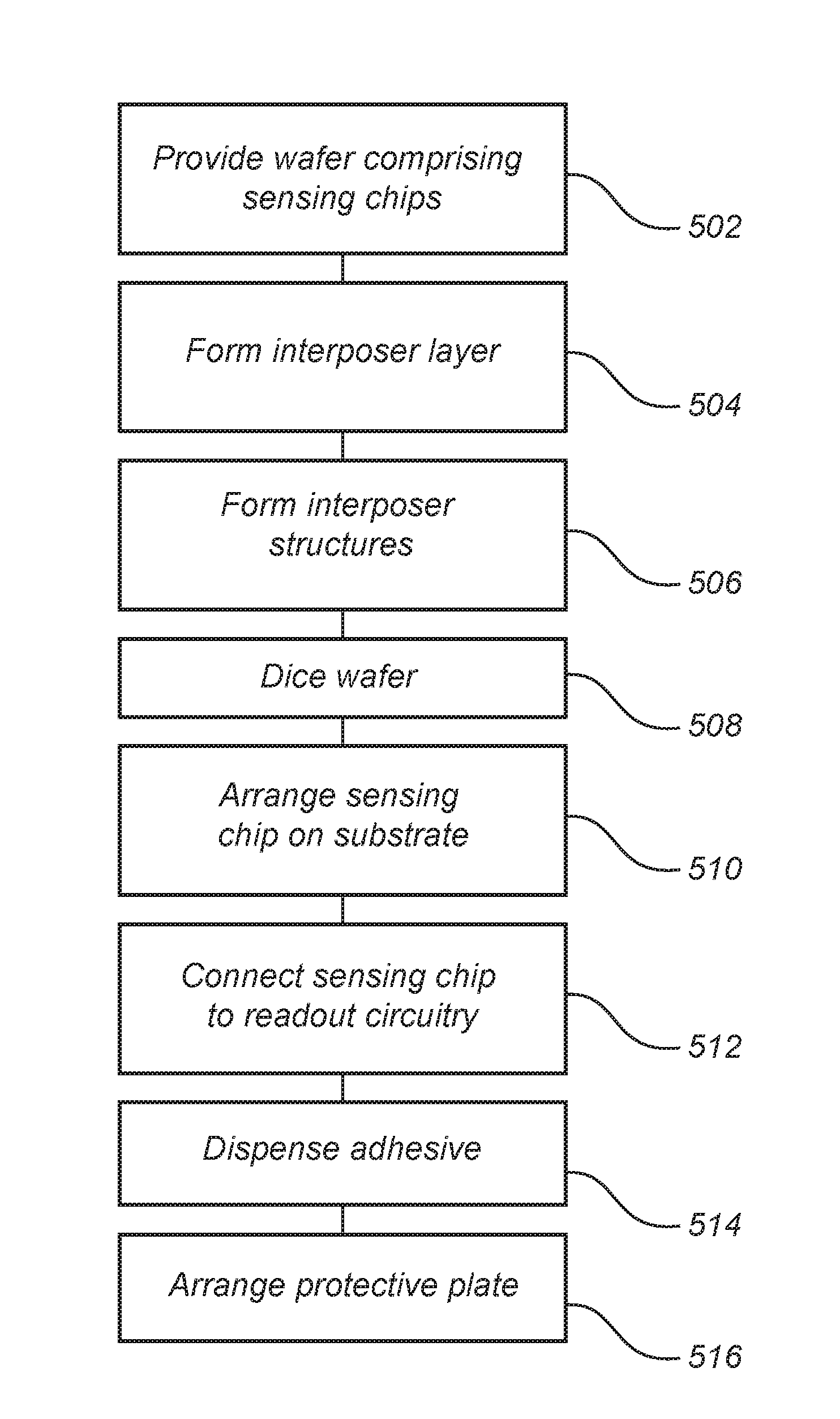
[0047]In the present detailed description, various embodiments of a fingerprint sensing device according to the present invention are mainly discussed with reference to a capacitive fingerprint sensing device. A method for manufacturing a fingerprint sensing device is also discussed.

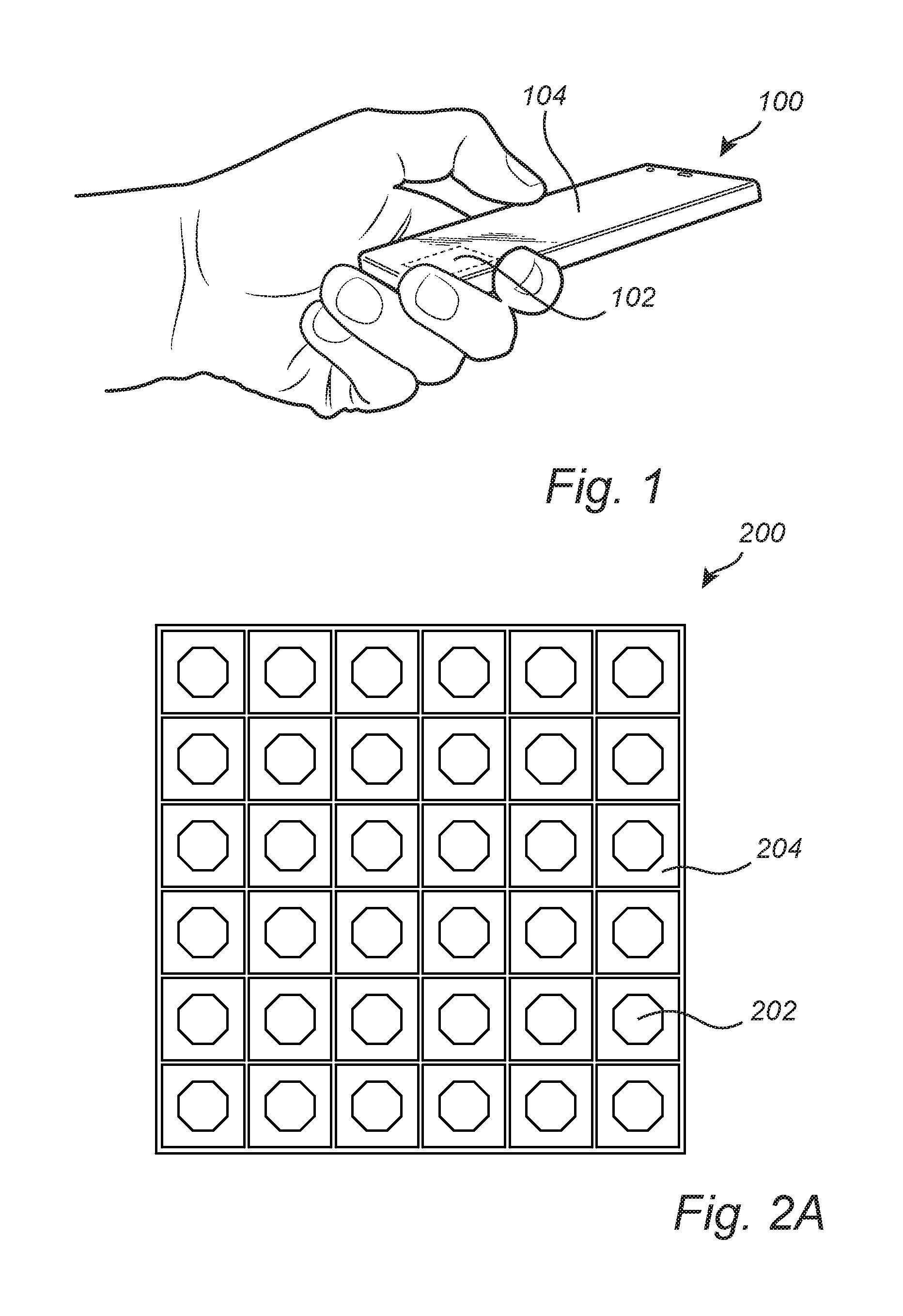
[0048]FIG. 1 is a schematic illustration of a handheld device 100 comprising a fingerprint sensing device 102 comprising a touchscreen display 104. A fingerprint sensing device 102 can be used in for example a mobile phone, a tablet computer, a portable computer or any other electronic device requiring a way to identify and / or authenticate a user.

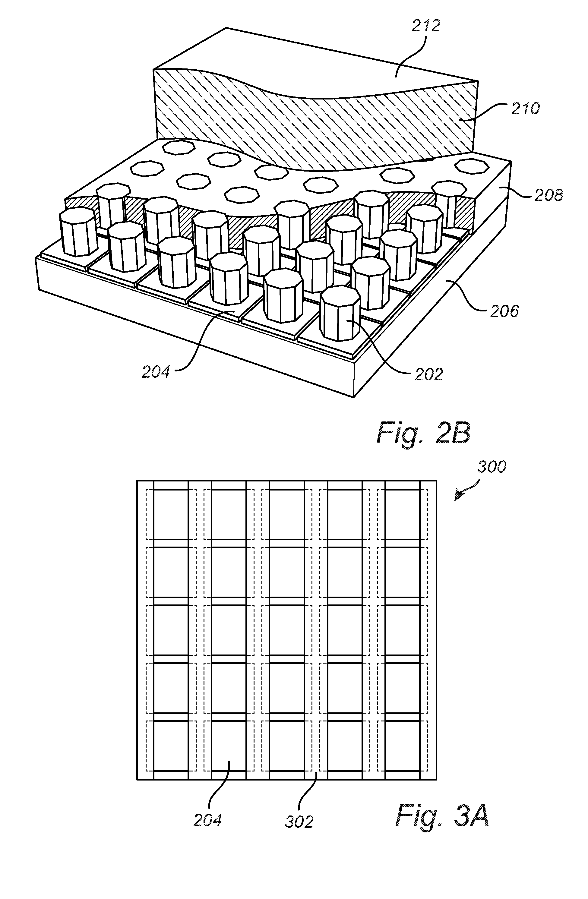
[0049]FIG. 2A is a schematic illustration of a fingerprint sensing device 200 according to an embodiment of the invention, as seen in a top view. In particular, FIG. 2A illustrates the outline of a plurality of interposer structures 202, where each interposer structure 202 is arranged on a sensing element 204 of the sensing device 200.

[0050]FIG. 2B illustrates t...


PUM


Abstract

The invention relates to a fingerprint sensing device comprising: a sensing chip comprising an array of sensing elements being configured to be connected to readout circuitry for detecting a capacitive coupling between each of the sensing elements and a finger placed on a sensing surface of the sensing device, wherein a surface of the sensing elements define a sensing plane; a plurality of interposer structures arranged on the sensing chip extending above sensing plane, wherein the plurality of interposer structures have substantially the same height above the sensing plane; and a protective plate attached to the sensing chip by means of an adhesive arranged on the sensing chip, wherein the protective plate rests on the interposer structures such that a distance between the protective plate and the sensing plane is defined by the height of the interposer structures.

Description

CROSS REFERENCE TO RELATED APPLICATIONS[0001]This application claims the benefit of Swedish Patent Application No. 1550748-6 filed Jun. 8, 2015, and Swedish Patent Application No. 1551288-2 filed Oct. 7, 2015. The disclosures of the above applications are incorporated herein by reference in their entirety.FIELD OF THE INVENTION[0002]The present invention relates to a fingerprint sensing device. In particular, the present invention is related to a fingerprint sensing device comprising an interposer structure for enhancing the performance in the sensing device, and to a method for manufacturing a fingerprint sensor comprising such an interposer structure.BACKGROUND OF THE INVENTION[0003]As the development of biometric devices for identity verification, and in particular of fingerprint sensing devices, has lead to devices which are made smaller, cheaper and more energy efficient, the possible applications for such devices are increasing.[0004]In particular fingerprint sensing has been ...

Claims


Application Information

Patent Timeline
Patent Type & Authority Applications(United States)
IPC IPC(8): G06K9/00G06F18/00G06V40/13
CPCG06K9/00053G06V40/1306G06V40/1329G03F7/16G06F18/00
Inventor LUNDAHL, KARL
Owner FINGERPRINT CARDS ANACATUM IP AB
Why Eureka
Try Eureka