Process for making plane floating grid and nonvolatile memory element containing same

A technology for memory components and manufacturing methods, applied in electrical components, semiconductor devices, semiconductor/solid-state device manufacturing, etc., can solve problems such as floating gate charge loss, interference, difficulty in obtaining windows for lithography and etching control gates

Inactive Publication Date: 2004-06-16
WINBOND ELECTRONICS CORP
View PDF0 Cites 1 Cited by
  • Summary
  • Abstract
  • Description
  • Claims
  • Application Information

AI Technical Summary

Problems solved by technology

But when the device size shrinks, it is difficult to get a window large enough to lithography and etch the control gate
Plus the acute angle of the floating gate 20 ( figure 2 indicated by the dotted circle of ) will raise the electric field

Method used


Image

  • Process for making plane floating grid and nonvolatile memory element containing same
  • Process for making plane floating grid and nonvolatile memory element containing same
  • Process for making plane floating grid and nonvolatile memory element containing same

Examples


Embodiment Construction

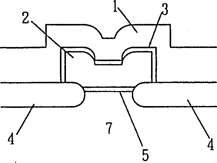
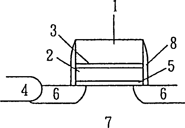
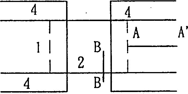
[0031] see Figure 4 , this figure shows a method for manufacturing a planar floating gate of the present invention, the steps of which include: forming an oxide layer SiO 2 After laying a layer of nitride layer Si 3 N 4 on the oxide layer. The developed nitride pattern is produced by lithography and etching, and the nitride residual area is the active area AA used to fabricate the components in the IC. Using residual Si 3 N 4 Nitride pattern as mask to etch away SiO 2 layer and etch the Si substrate to form trenches. An oxide layer is formed on the surface of the trench 14 and deposited to fill the trench. The oxide on the surface of the wafer is polished by using the oxide chemical mechanical polishing (CMP) with the nitride layer as the polishing stop layer. Etch the oxide layer to the height of the active area (AA) Si surface. The remaining nitride pattern and oxide on the silicon surface are then removed. Oxide-filled trench isolation is called STI (Shallow Tren...


PUM


Abstract

The invention relates to a plane floating grid making method, mainly including: deposit oxide between polycrystal silicon layers to cover the wafer surface; open the floating grid region (except extension part) and etching oxide between partial polycrystal silicon layers; open all the floating regions (except extension part) and all the active regions. It can make an approximate 'T' floating grid with flat and wide surface and coupled area with the control grid. It also relates to a construction of involatile memory component with the plane floating grid by the making method.

Description

(1) Technical field [0001] The present invention relates to a manufacturing method and structure of a planar floating gate, in particular to a manufacturing method and structure of a non-volatile memory device having a floating gate with a wide and flat surface. (2) Background technology [0002] Recently, the integrated circuit IC gradually develops towards the direction of small size and high density, and the size of both vertical and parallel planes is reduced at the same time. In the process of changing the size of the device, the process control window and the properties of the device will be affected to some extent, especially the non-volatile memory (Non-Volatile Memory, NVM) technology is deeply affected by the shrinking of the size of the IC device. For example, the most common is a non-volatile memory (NVM) device formed by stacking two polysilicon layers together. The conventional non-volatile memory (NVM) element is shown in Figures 1(a) to 1(c), wherein Figure ...

Claims


Application Information

Patent Timeline
IPC IPC(8): H01L21/28H01L21/82
Inventor 张文岳
Owner WINBOND ELECTRONICS CORP
Why Eureka
Try Eureka