Digital manufacture of an electrical circuit

a digital manufacturing and electrical circuit technology, applied in electrography/magnetography, resistive material coating, metallic pattern materials, etc., can solve the problems of high initial cost and much more layout effor

Inactive Publication Date: 2011-03-31
EASTMAN KODAK CO
View PDF8 Cites 5 Cited by
  • Summary
  • Abstract
  • Description
  • Claims
  • Application Information

AI Technical Summary

Benefits of technology

[0018]In view of the above, this invention is directed to electrographic printing wherein toner and / or laminates form one or more multi-channeled layers, with a particular pattern, which can be printed by electrographic techniques and then filled or adapted as needed. Such electrographic printing includes the steps of forming a desired image, electrographically, on a receiver member and incorporating channels that are embedded into the design.
[0019]The multi layered channel printing apparatus and related method and print incorporates one or more static layers, and one or more layers that allow a variety of fluids to move into and / or through the micro channels via an opening or through a direct fill. These fluids can be solidified or left as a fluid. An optional capping layer or substrate may then also be applied as well as post printing treatments.
[0020]The printing method for producing a digital specialty item, such as upon a receiver, includes the steps of depositing a static layer of material, such as toner, to form a predetermined base layer, depositing one or more material nodes over the static layer, the material nodes in a first state and depositing a top layer of material over the nodes, the top layer defining an expansion space between the static layer and the top layer so that during activation the one or more nodes can change in the expansion space to create a predetermined digitally prepared specialty item.
[0021]The invention, and its objects and advantages, will become more apparent in the detailed description presented below.

Problems solved by technology

They require much more layout effort and higher initial cost than either wire-wrapped or point-to-point constructed circuits, but are much cheaper and faster for high-volume production.

Method used


Image

  • Digital manufacture of an electrical circuit
  • Digital manufacture of an electrical circuit
  • Digital manufacture of an electrical circuit

Examples


Embodiment Construction

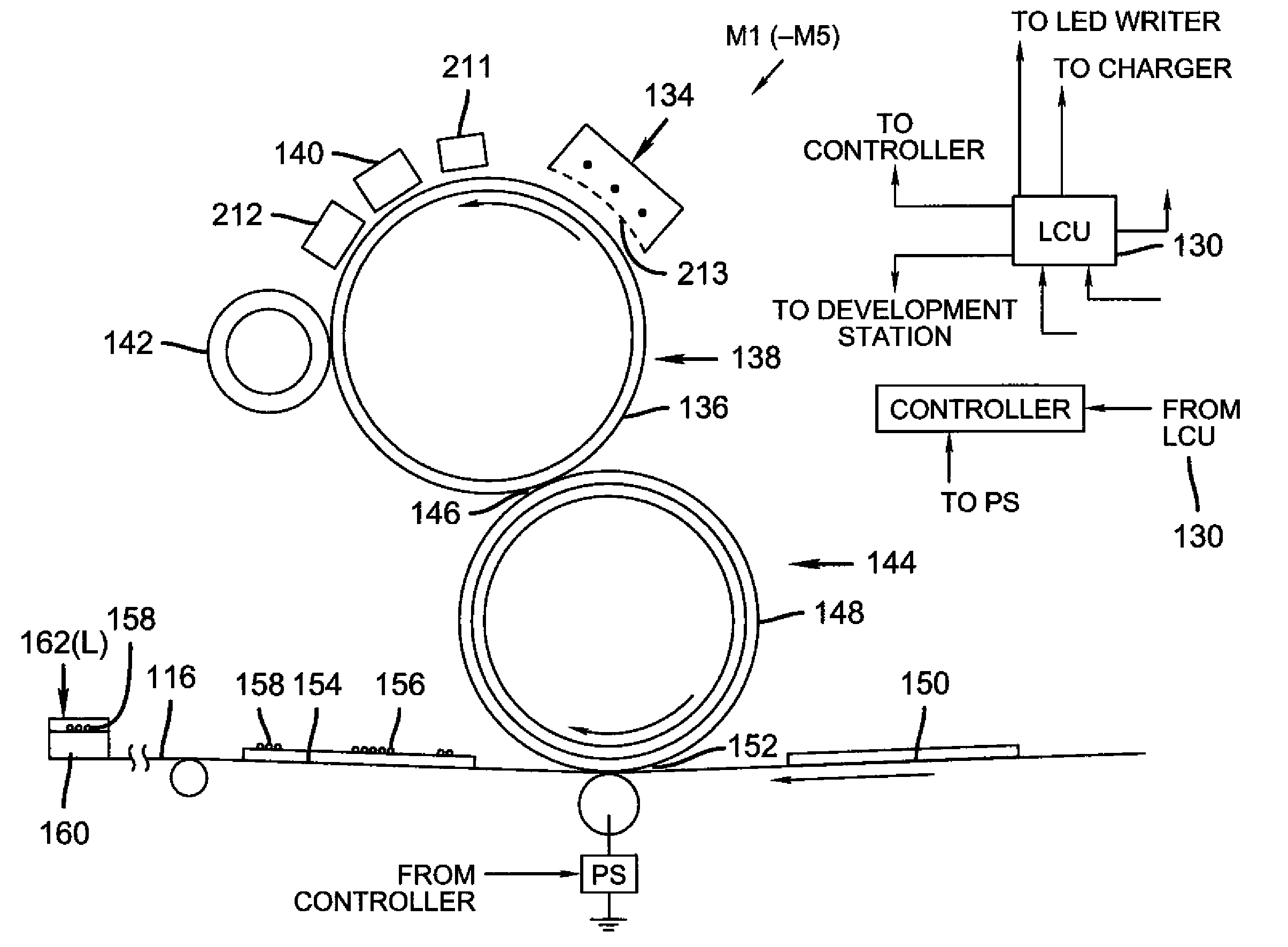
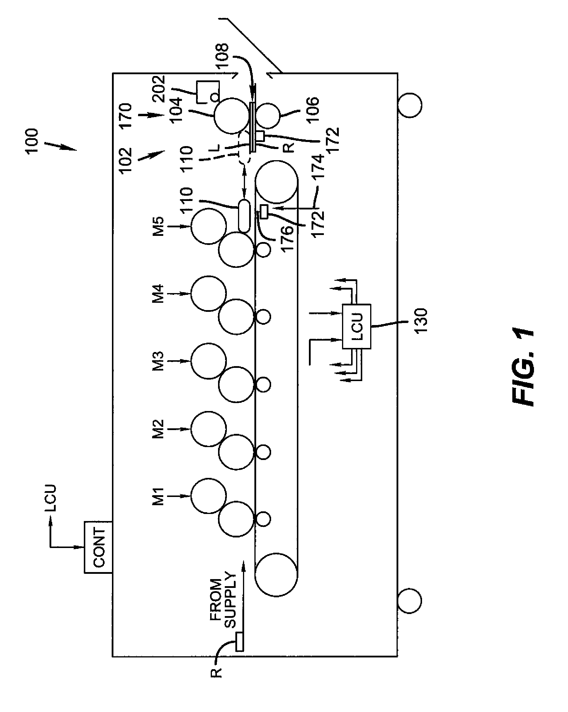
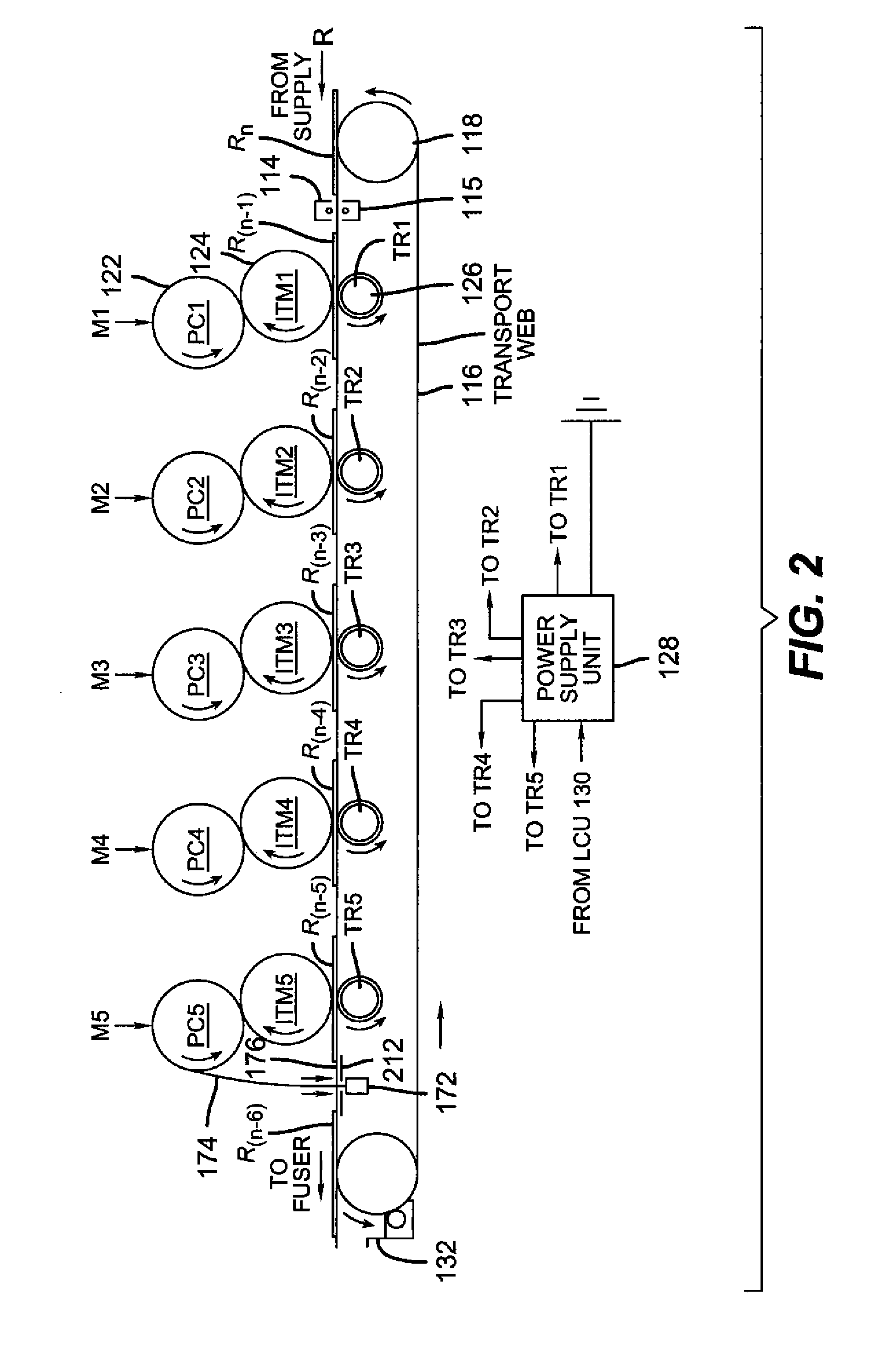
[0033]Referring now to the accompanying drawings, FIGS. 1 and 2 are side elevational views schematically showing portions of a typical electrographic print engine or printer apparatus suitable for printing of multi-channel layered prints. One embodiment of the invention involves printing using an electrophotographic engine having five sets of single layer image producing or printing stations or modules arranged in tandem and an optional finishing assembly. The invention contemplates that more or less than five stations may be combined to deposit a material, such as toner, on a single receiver member, or may include other typical electrographic writers, printer apparatus, or other finishing devices.

[0034]In one embodiment, an electrographic printer apparatus 100 has a number of tandemly arranged electrostatographic image forming printing modules M1, M2, M3, M4, and M5 and a finishing assembly 102. Additional modules may be provided.

[0035]Each of the printing modules generates a singl...


PUM

PropertyMeasurementUnit
volume average diameteraaaaaaaaaa
specific gravityaaaaaaaaaa

Abstract

The electrographic printing of one or more multi-channeled layers having a particular pattern by electrographic techniques that produces a specialty item electrographically. Such electrographic printing comprises the steps of forming a desired print image, electrographically, on a receiver member utilizing predetermined sized marking particles; and, where desired, forming one or more final multi-channeled layers utilizing marking particles of a predetermined size or size distribution.

Description

CROSS REFERENCE TO RELATED APPLICATIONS[0001]This application relates to commonly assigned, copending U.S. application Ser. No. ______ (Docket No. 95803DPS), filed ______, entitled: “DIGITAL MANUFACTURE OF A MULTI-CHANNELED SPECIALITY ITEM.”FIELD OF THE INVENTION[0002]The present invention relates electrographic printing and more particularly to printing an electrical circuit electrographically.BACKGROUND OF THE INVENTION[0003]A printed circuit board is used to mechanically support and electrically connect electronic components using conductive pathways, or traces, etched from copper sheets laminated onto a non-conductive substrate. They may also be referred to as printed wiring board or etched wiring board. A printed circuit populated with electronic components is a printed circuit assembly, also known as a printed circuit board assembly.[0004]Printed circuits are rugged, inexpensive, and can be highly reliable. They require much more layout effort and higher initial cost than eith...

Claims


Application Information

Patent Timeline
Patent Type & Authority Applications(United States)
IPC IPC(8): H05K1/09G03G15/22G03G13/20
CPCG03G15/1625H05K1/0272H05K3/101H05K2203/0517H05K3/1266H05K3/4664H05K3/107
Inventor SUCHY, DONNA P.HERRICK, DIANE M.
Owner EASTMAN KODAK CO
Why Eureka
Try Eureka