Liquid crystal display device and electronic device including the liquid crystal display device

Active Publication Date: 2011-04-21
SEMICON ENERGY LAB CO LTD
View PDF99 Cites 119 Cited by
  • Summary
  • Abstract
  • Description
  • Claims
  • Application Information

AI Technical Summary

Benefits of technology

[0015]In a pixel including a thin film transistor using an oxide semiconductor, the off-state current can be reduced. Therefore, a liquid crystal display device capable of extending the period in which a storage capacitor can hold a volta

Problems solved by technology

On the other hand, thin film transistors manufactured using crystalline silicon have high field effect mobility, but due to a crysta

Method used


Image

  • Liquid crystal display device and electronic device including the liquid crystal display device
  • Liquid crystal display device and electronic device including the liquid crystal display device
  • Liquid crystal display device and electronic device including the liquid crystal display device

Examples


embodiment 1

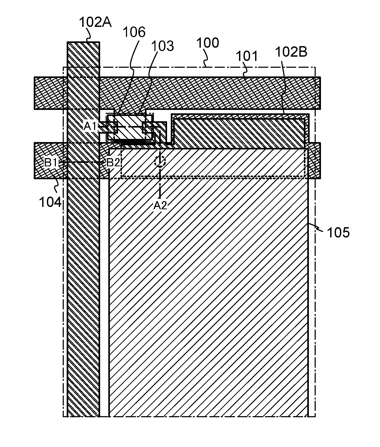
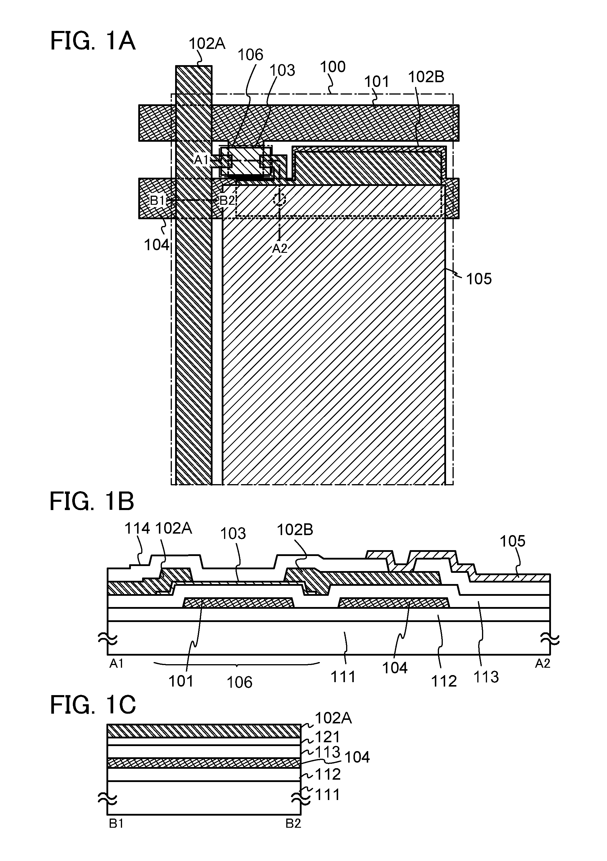
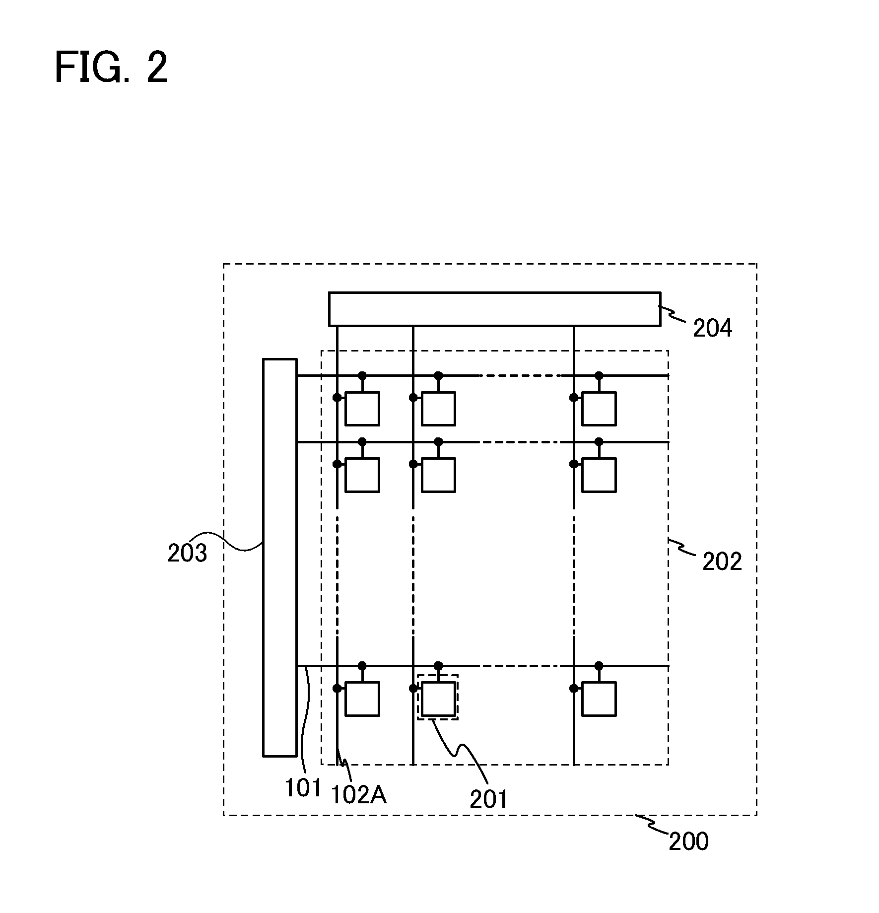
[0049]An example is described below in which a pixel of a liquid crystal display device is formed using a thin film transistor. In this embodiment, a thin film transistor (hereinafter also referred to as a TFT) included in a pixel of a liquid crystal display device, and an electrode functioning as a pixel electrode connected to the TFT (simply also referred to as a pixel electrode) are described as examples. Note that a pixel refers to an element group which includes elements provided in each pixel of a display device, for example, an element for controlling display in accordance with electric signals, such as a thin film transistor, an electrode functioning as a pixel electrode, or a wiring. Note that a pixel may include a color filter and the like, and may correspond to one color component whose brightness can be controlled with one pixel. Therefore, for example, in the case of a color display device including color components of R, G, and B, a minimum unit of an image includes th...

embodiment 2

[0087]In this embodiment, an example of a thin film transistor which can be applied to a liquid crystal display device described in this specification will be described. A thin film transistor 410 described in this embodiment can be used as the thin film transistor 106 of Embodiment 1.

[0088]A thin film transistor of this embodiment and an embodiment of a method for manufacturing the thin film transistor are described using FIGS. 5A and 5B and FIGS. 6A to 6E.

[0089]FIG. 5A illustrates an example of a planar structure of the thin film transistor, and FIG. 5B illustrates an example of a cross-sectional structure thereof. The thin film transistor 410 shown in FIGS. 5A and 5B is a top-gate thin film transistor.

[0090]FIG. 5A is a plan view of the top-gate thin film transistor 410 and FIG. 5B is a cross-sectional view along line C1-C2 in FIG. 5A.

[0091]The thin film transistor 410 includes, over a substrate 400 having an insulating surface, an insulating layer 407, an oxide semiconductor lay...

embodiment 3

[0157]In this embodiment, another example of a thin film transistor which can be applied to a liquid crystal display device disclosed in this specification will be described. Note that Embodiment 2 can be referred to for the same portions as and the portions and steps having functions similar to those in Embodiment 2, and description thereof is not repeated. Further, a specific description for the same portions is omitted. A thin film transistor 460 described in this embodiment can be used as the thin film transistor 106 of Embodiment 1.

[0158]A thin film transistor of this embodiment and an embodiment of a method for manufacturing the thin film transistor are described using FIGS. 7A and 7B and FIGS. 8A to 8E.

[0159]FIG. 7A illustrates an example of a planar structure of the thin film transistor, and FIG. 7B illustrates an example of a cross-sectional structure thereof. The thin film transistor 460 shown in FIGS. 7A and 7B is a top-gate thin film transistor.

[0160]FIG. 7A is a plan vi...


PUM


Abstract

In a liquid crystal display device including a plurality of pixels in a display portion and configured to performed display in a plurality of frame periods, each of the frame periods includes a writing period and a holding period, and after an image signal is input to each of the plurality of pixels in the writing period, a transistor included in each of the plurality of pixels is turned off and the image signal is held for at least 30 seconds in the holding period. The pixel includes a semiconductor layer including an oxide semiconductor layer, and the oxide semiconductor layer has a carrier concentration of less than 1×10¹⁴/cm3.

Description

TECHNICAL FIELD[0001]An embodiment of the present invention relates to a liquid crystal display device. An embodiment of the present invention relates to an electronic device including the liquid crystal display device.BACKGROUND ART[0002]Thin film transistors formed over a flat plate such as a glass substrate have been manufactured using amorphous silicon or polycrystalline silicon, as typically seen in liquid crystal display devices. Thin film transistors manufactured using amorphous silicon have low field effect mobility but can be formed over a large glass substrate. On the other hand, thin film transistors manufactured using crystalline silicon have high field effect mobility, but due to a crystallization step such as laser annealing, such a transistor is not necessarily suitable for being formed over a large glass substrate.[0003]In view of the foregoing, attention has been drawn to a technique by which a thin film transistor is manufactured using an oxide semiconductor, and s...

Claims


Application Information

Patent Timeline
IPC IPC(8): G09G5/00G09G3/36
CPCG09G3/3648G09G2300/08H01L29/7869H01L27/1225H01L29/06G09G3/3614G09G3/3677G09G2310/0286G09G2310/08G09G2330/021H01L21/02164H01L21/02266H01L21/02565H01L21/02631H01L21/467H01L21/477H01L27/1255H01L29/24H01L29/42356H01L29/45H01L29/66969H01L29/78648G02F1/133553G02F1/13439G02F1/1368G02F2201/123G02F2202/10
Inventor YAMAZAKI, SHUNPEIARASAWA, RYOKOYAMA, JUNTSUBUKU, MASASHINODA, KOSEI
Owner SEMICON ENERGY LAB CO LTD
Why Eureka
Try Eureka