Touch display panel and touch sensing unit thereof

a touch display panel and touch sensing technology, applied in the field of touch display panel and touch sensing unit thereof, can solve the problems of affecting the yield of the touch panel, the aperture ratio of the touch display panel is reduced, and the input signal of the touch cannot be easily identified, so as to achieve the effect of negligible effects on the aperture ratio of the touch display panel

Active Publication Date: 2011-04-28
AU OPTRONICS CORP
View PDF7 Cites 32 Cited by
  • Summary
  • Abstract
  • Description
  • Claims
  • Application Information

AI Technical Summary

Benefits of technology

[0009]The touch display panel in accordance to the present invention utilizes non-transparent bridge lines of a high electrical conductivity to connect with the first transparent sensing pads so that the touch sensitivity of the touch sensing unit of the touch display panel is improved. Since the line width of each of the non-transparent bridge lines is substantially between 0.5 micrometers and 10 micrometers, the non-transparent bridge lines contribute negligible effects on the aperture ratio of the touch display panel.

Problems solved by technology

The transparent sensing pads are made of a transparent conductive material, but the transparent conductive material has a higher resistance so that the touch input signals cannot be easily identified when the transparent conductive material is applied in a large size touch panel.
However, since the metallic bridge line is made of a non-transparent material, the metallic bridge line would cause the aperture ratio of the touch display panel to decrease when the line width of the metallic bridge line is too broad.
In addition, during the fabrication of the metallic bridge lines of conventional touch panels, breakages of the metallic bridge lines often occur due to over etching, and thereby the breakages affect the yields of the touch panels.

Method used


Image

  • Touch display panel and touch sensing unit thereof
  • Touch display panel and touch sensing unit thereof
  • Touch display panel and touch sensing unit thereof

Examples


Embodiment Construction

[0017]To provide a better understanding of the present invention, preferred embodiments will be detailed as follows. The preferred embodiments of the present invention are illustrated in the accompanying drawings with numbered elements to elaborate the contents and effects to be achieved.

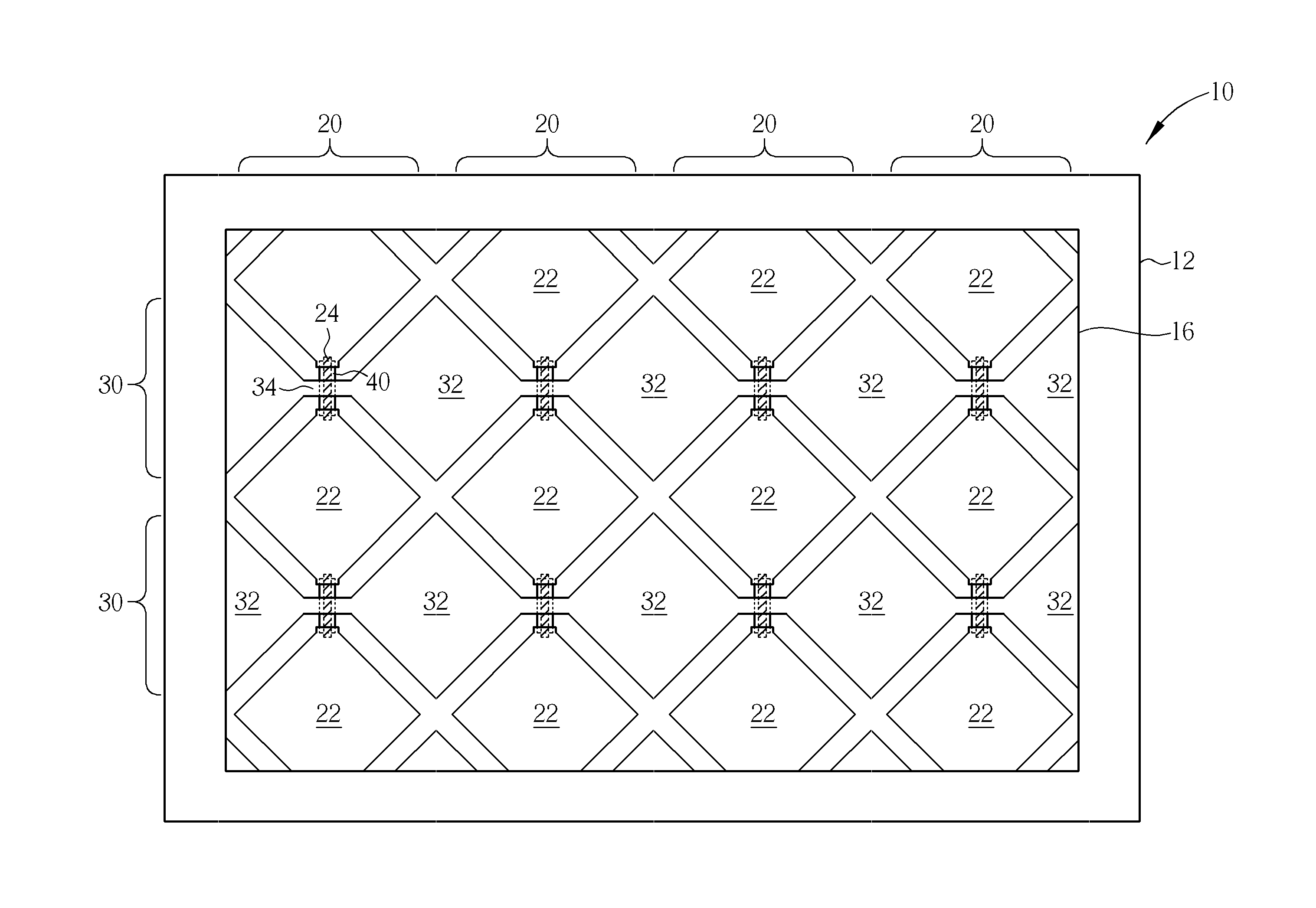
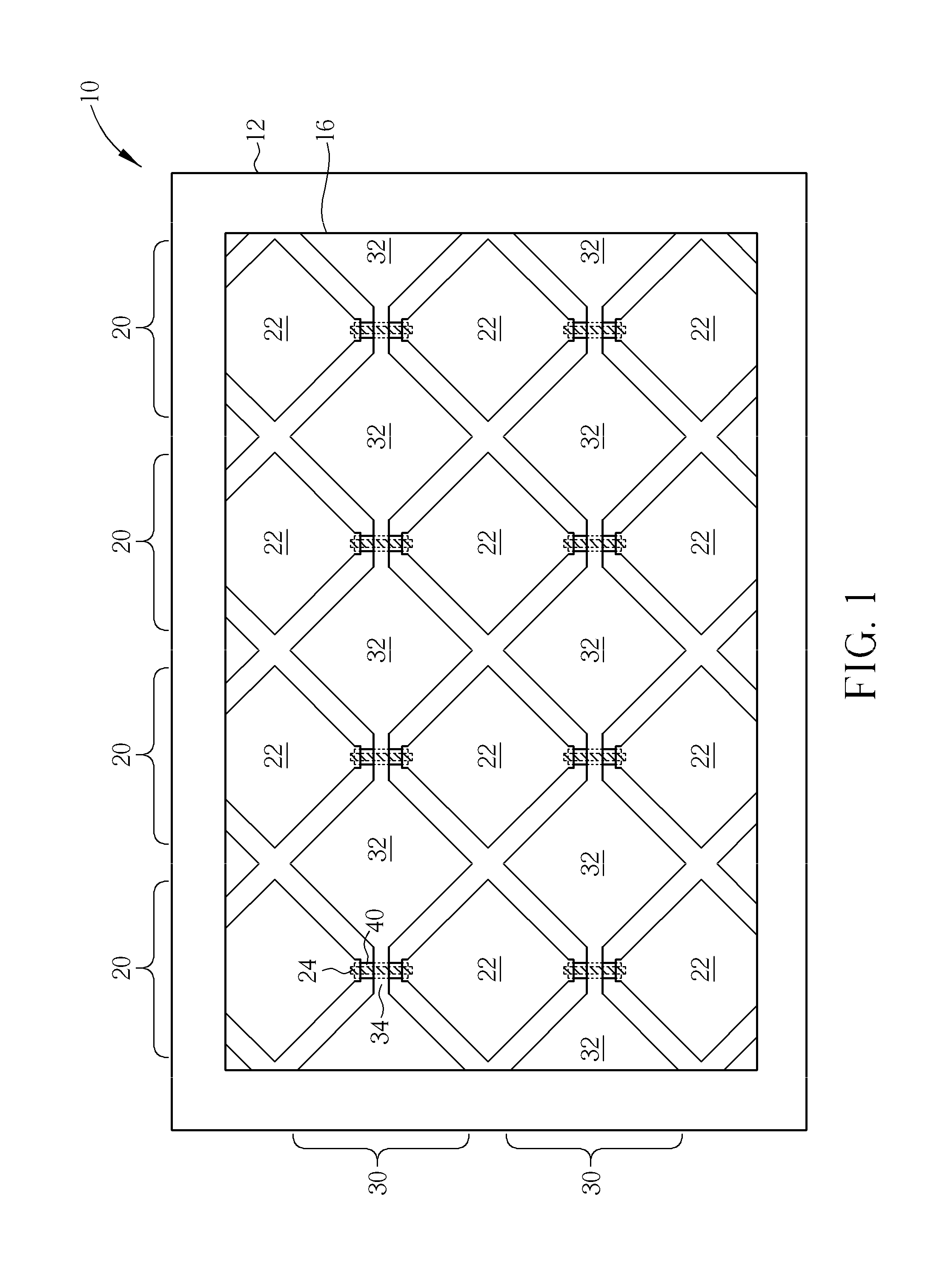
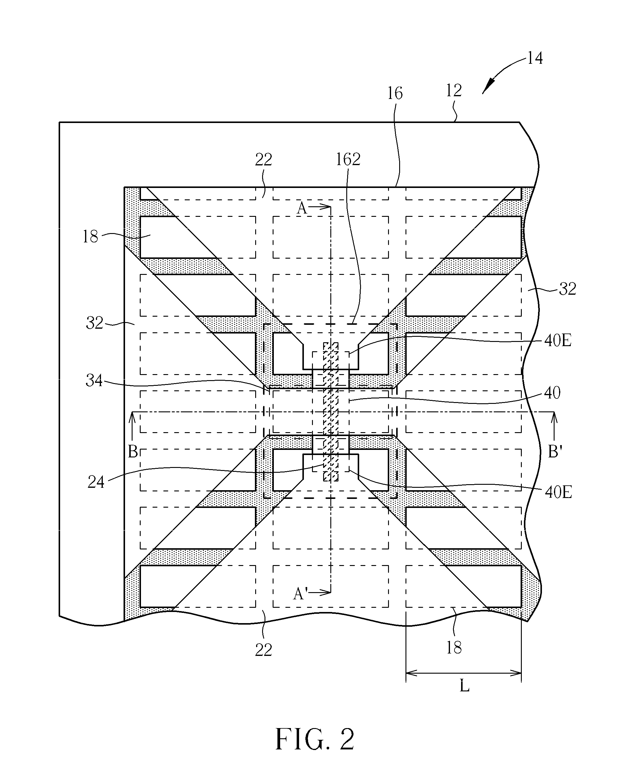
[0018]Referring to FIG. 1 to FIG. 4, FIG. 1 to FIG. 4 are schematic diagrams illustrating a touch display panel of a preferred embodiment in accordance to the present invention. FIG. 1 is a schematic top view diagram in accordance to the touch display panel of the present embodiment. FIG. 2 is a schematic zoom-in diagram of the touch sensing unit in accordance to the touch display panel of the present embodiment. FIG. 3 is a schematic cross-sectional diagram of the touch sensing unit in accordance to the touch display panel of the present embodiment along line A-A′. FIG. 4 is a schematic cross-sectional diagram of the touch sensing unit in accordance to the touch display panel of the present embodim...


PUM


Abstract

A touch display panel includes a display panel and a touch sensing unit. The touch sensing unit includes first sensing series, and second sensing series. Each of the first sensing series includes a plurality of first transparent sensing pads disposed along a first direction, and a plurality of non-transparent bridge lines disposed along the first direction. Each of the non-transparent bridge lines is disposed between two adjacent first transparent sensing pads, overlapping with two adjacent first transparent sensing pads, and electrically connected to two adjacent first transparent sensing pads. The line width of each non-transparent bridge line is substantially between 0.5 micrometers and 10 micrometers, and the reduction of aperture ratio in a pixel region of the touch display panel caused by the non-transparent bridge lines is substantially between 0.1% and 5%.

Description

BACKGROUND OF THE INVENTION[0001]1. Field of the Invention[0002]The present invention relates to a touch display panel and a touch sensing unit thereof, and more particularly to a touch display panel with non-transparent bridge lines of a high electrical conductivity electrically connected to transparent conductive pads, and a touch sensing unit thereof. The line width of each of the non-transparent bridge lines is substantially between 0.5 micrometer and 10 micrometers, and an aperture ratio of pixel regions of the touch display panel occupied by the non-transparent bridge lines is substantially between 0.1% and 5%.[0003]2. Description of the Prior Art[0004]In present consumer electronics, tablet personal computers, personal digital assistants (PDA), mobile phones, global positioning systems (GPS), multimedia players and other portable electronic devices widely apply touch panels to replace conventional keyboards as the data communicational interface between human and the electroni...

Claims


Application Information

Patent Timeline
Patent Type & Authority Applications(United States)
IPC IPC(8): G06F3/045
CPCG06F2203/04111G06F3/044G06F3/0443G06F3/0446
Inventor LEE, HSIN-HUNGCHEN, PEI-YUCHIU, YU-MEICHANG, WEI-JENLIN, YU-CHUANCHENG, KUO-HSING
Owner AU OPTRONICS CORP
Why Eureka
Try Eureka