Cache system

a technology of cache system and cache, applied in the field of cache system, can solve the problems of complex control of system, inability to determine the maximum error number in advance, and difficulty in realizing the system

Inactive Publication Date: 2011-05-05
RENESAS ELECTRONICS CORP
View PDF8 Cites 4 Cited by
  • Summary
  • Abstract
  • Description
  • Claims
  • Application Information

AI Technical Summary

Benefits of technology

[0015]In the present invention, a correctable error occurrence condition is newly provided as an additional condition to a block to which a dirty determining

Problems solved by technology

In addition, although it is required to latch error addresses, the maximum latch number of addresses, that is, the maximum error number cannot be determined in advance.
Accordingly, there is a problem that the m

Method used


Image

  • Cache system
  • Cache system
  • Cache system

Examples


first embodiment

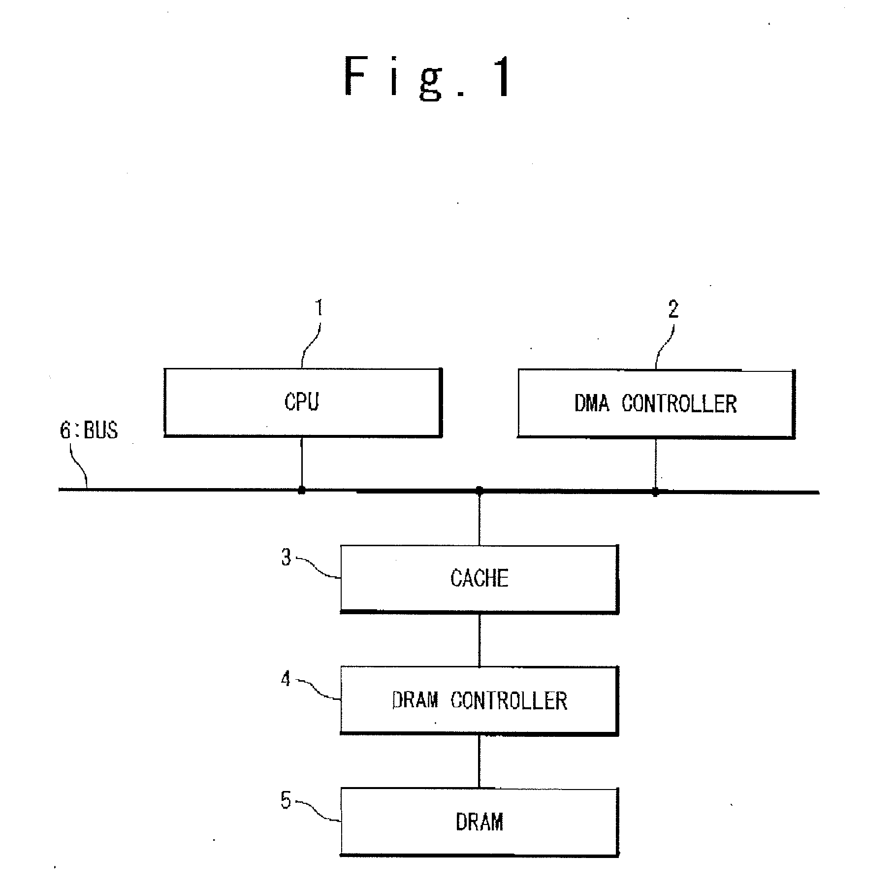
[0024]In a first embodiment of the present invention, a case where a CPU 1 is of a single-core type will be described. FIG. 1 is a block diagram showing the configuration of a cache system according to the present embodiment. The cache system includes a CPU 1, a DMA controller 2, a cache 3, a DRAM controller 4, a DRAM 5 as a main memory, and a bus 6.

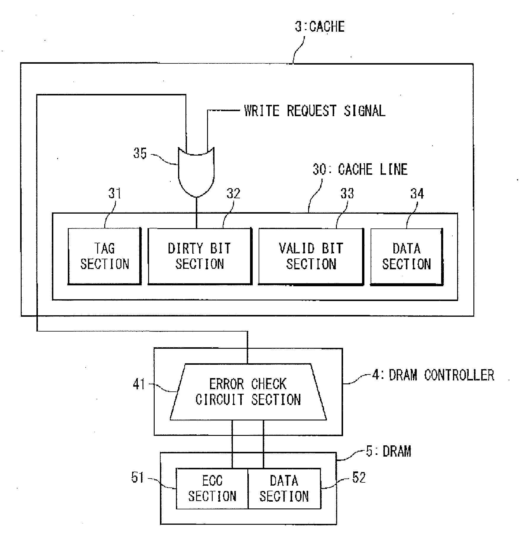
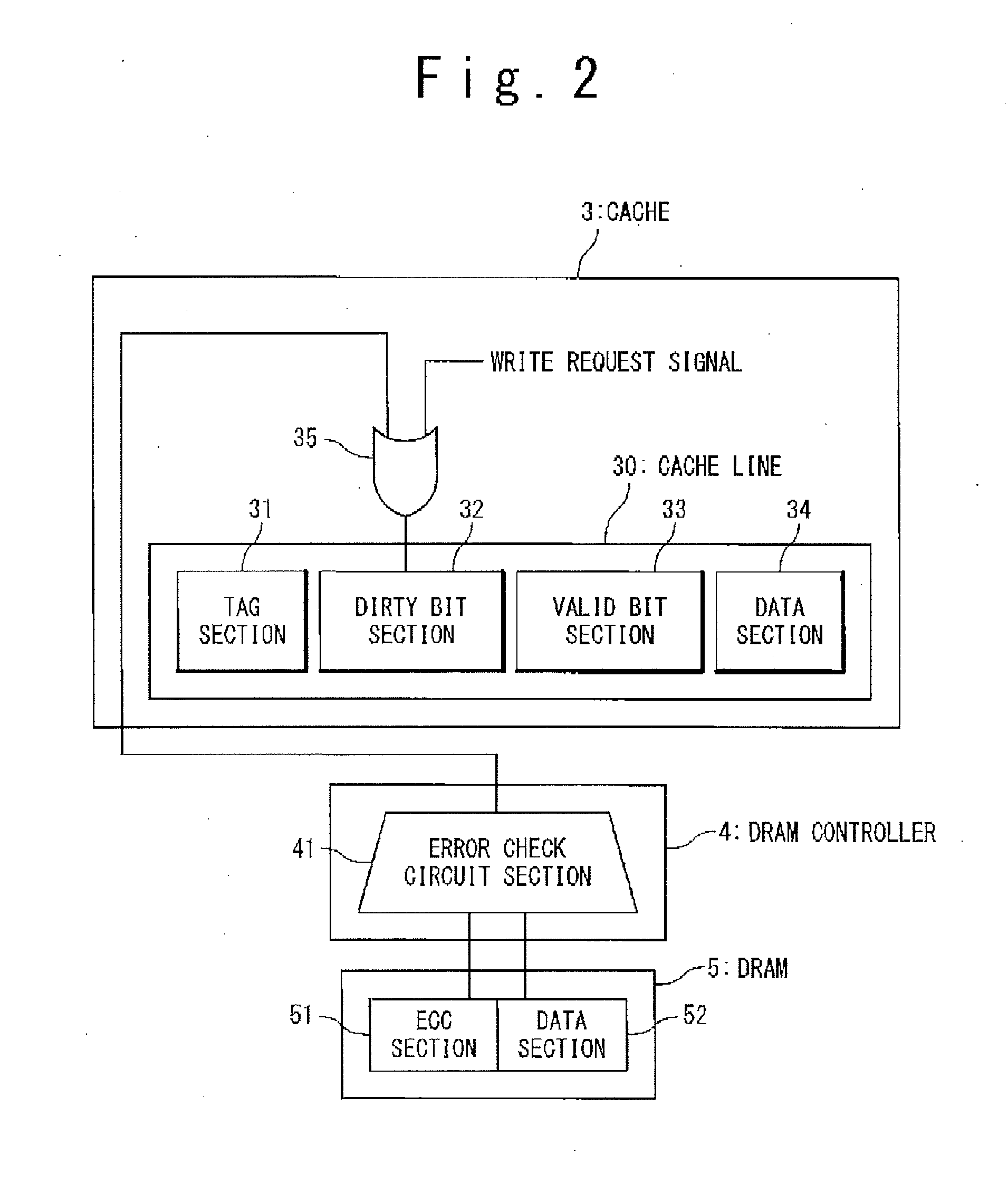
[0025]FIG. 2 is a detailed block diagram shoving the configurations of the cache 3, the DRAM controller 4, and the DRAM 5 according to the present embodiment. The cache 3 includes cache lines 30 and an OR calculation circuit 35. The number of cache lines 30 may be one or more. The cache line 30 includes a tag section 31, a dirty bit section 32, a valid bit-section 33, and a data section 34. The DRAM controller 4 includes an error check circuit 41. The DRAM 5 includes an ECC section 51 and a data section 52.

[0026]The respective sections in the cache line 30 will be described. When the cache line 30 caches a data as a cache data, a main bo...

second embodiment

[0052]In a second embodiment of the present, invention, a case that CPU is of multi-core to have CPUs 1-1 and 1-2 will be described.

[0053]FIG. 5 is a block diagram showing a configuration of the cache system according to the present embodiment. The cache system includes the first and second CPUs 1-1 and 1-2, first and second DMA controllers 2-1 and 2-2, first and second caches 3-1 and 3-2, the DRAM controller 4, the DRAM 5, and three busses 60, 60-1, and 60-2.

[0054]It should be noted that the configuration of the cache system shown in FIG. 5 is employed when the CPU is of multi cores CPUs 1-1 and 1-2, and the cache system according to the present embodiment can be attained even in a case of the multi-core of many CPUs. However, in this case, it is needless to say that a total number of the DMA controllers, the caches, and the buses need to be arbitrarily increased and decreased depending on the total number of the CPUs. Here, the case of two CPUs 1-1 and 1-2 will be described.

[0055]...


PUM


Abstract

A write-back cache system includes: a dirty bit section configured to store a dirty indication data indicating that cache data is in a dirty state; and an OR calculation circuit connected with a front-stage to the dirty bit section. The OR calculation circuit includes: a first input node configured to receive a write request signal indicating a write request of a cache data; a second input node configured to receive a correctable error determination signal of the cache data indicating that a correctable error is present in the cache data; and an output node configured to output a signal such that the dirty indication data is stored in the dirty bit section, when receiving at least, one of the write request signal and the correctable error determination signal.

Description

INCORPORATION BY REFERENCE[0001]This patent application claims a priority on convention based on Japanese Patent Application No. 2009-254095 filed on Nov. 5, 2009. The disclosure thereof is incorporated herein by reference.TECHNICAL FIELD[0002]The present invention relates to a cache system and a cache method using the cache system, and especially relates to a write-back type cache system and a cache method using the cache system.BACKGROUND ART[0003]In recent years, attention is focused on a problem of a soft error in a computer system with increase of a capacity of a main memory and miniaturization in a semiconductor process. For this reason, an ECC (Error Check and Correct) circuit is provided for reliability improvement, to perform correction of a 1-bit error and only detection of multi-bit error in case of memory read.[0004]However, when a memory data in which the 1-bit error has occurred, is left without being corrected, there is a possibility that the 1-bit error of the memory...

Claims


Application Information

Patent Timeline
IPC IPC(8): G06F11/07
CPCG06F11/0751G06F11/073
Inventor NAKATSUKA, HIROYASU
Owner RENESAS ELECTRONICS CORP
Why Eureka
Try Eureka