Transistors, methods of manufacturing a transistor and electronic devices including a transistor

a manufacturing method and transistor technology, applied in the direction of transistors, semiconductor devices, electrical devices, etc., can solve the problem that the characteristics of a transistor having an oxide layer as a channel layer may not be maintained constant (or consistently)

Active Publication Date: 2011-05-12
SAMSUNG ELECTRONICS CO LTD
View PDF9 Cites 43 Cited by
  • Summary
  • Abstract
  • Description
  • Claims
  • Application Information

AI Technical Summary

Problems solved by technology

However, the characteristics of a transistor having an oxide layer as a channel layer may not be constantly (or consistently) maintained because the oxide layer is sensitive to light.

Method used


Image

  • Transistors, methods of manufacturing a transistor and electronic devices including a transistor
  • Transistors, methods of manufacturing a transistor and electronic devices including a transistor
  • Transistors, methods of manufacturing a transistor and electronic devices including a transistor

Examples


Embodiment Construction

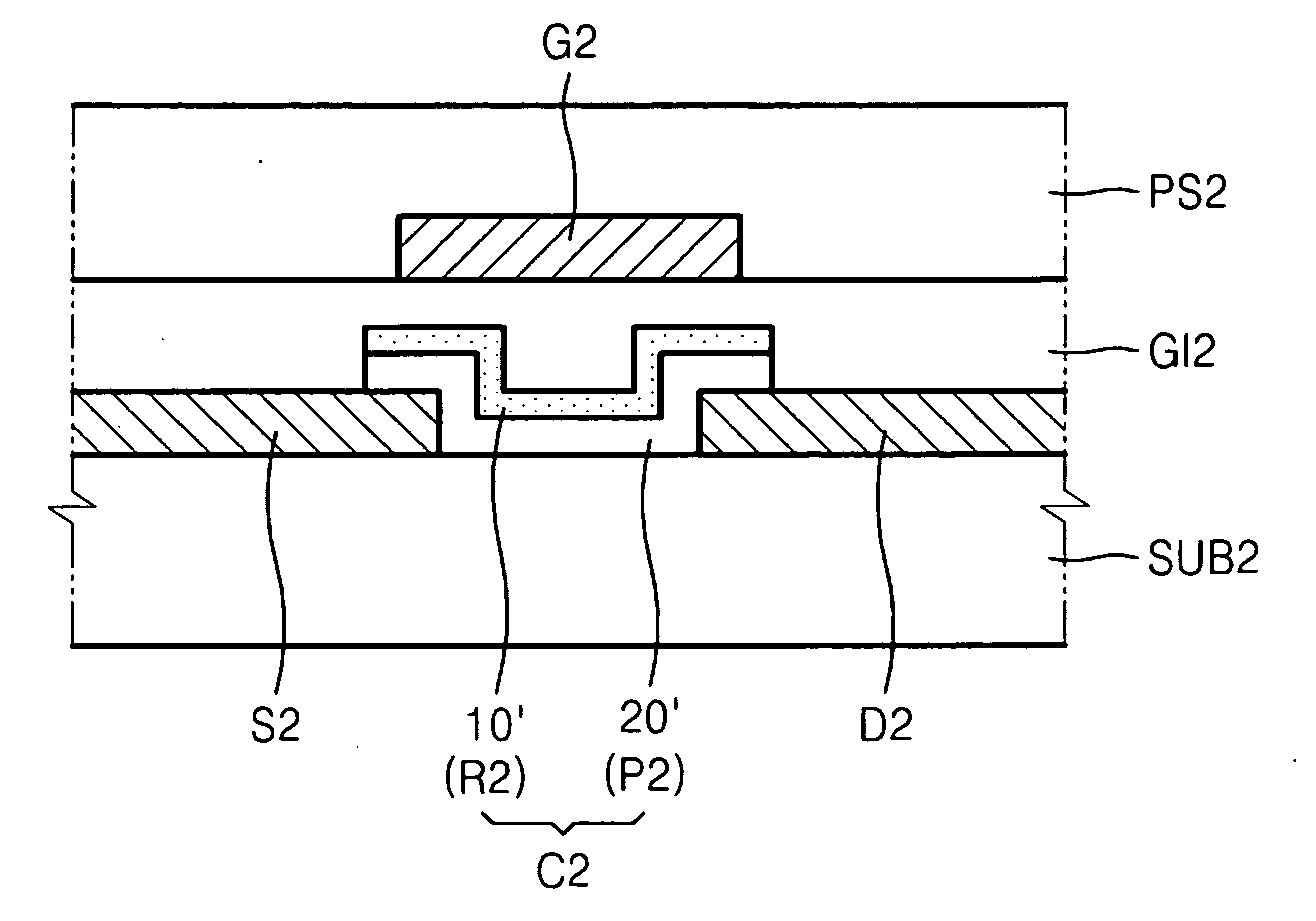
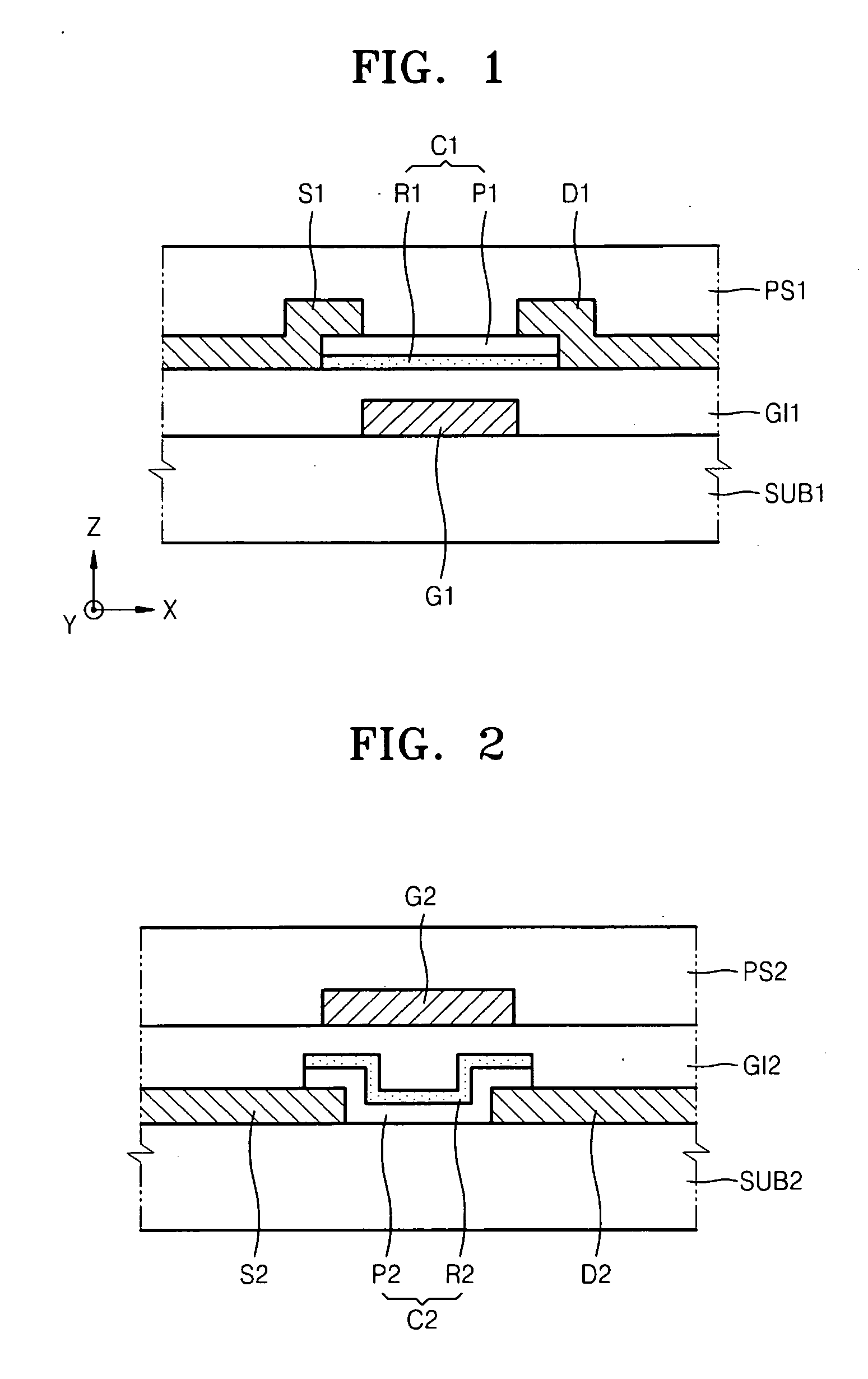
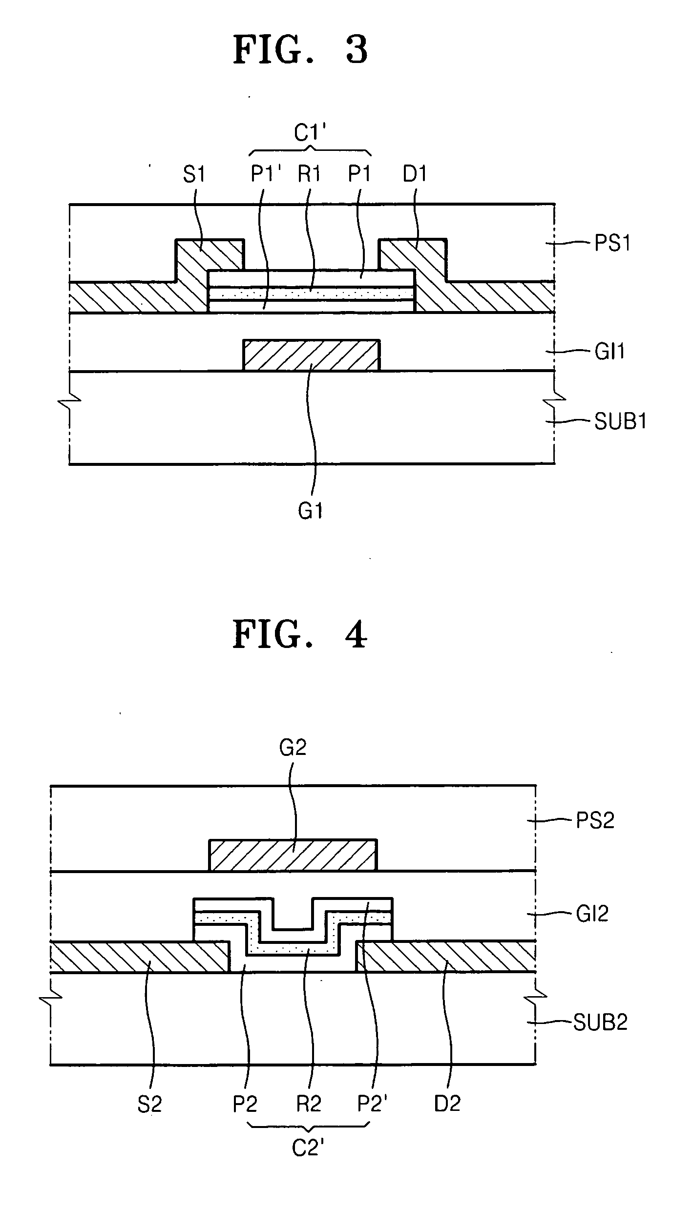
Various embodiments will now be described more fully with reference to the accompanying drawings in which some embodiments are shown.

Detailed illustrative embodiments are disclosed herein. However, specific structural and functional details disclosed herein are merely representative for purposes of describing embodiments. This invention may, however, may be embodied in many alternate forms and should not be construed as limited to only the embodiments set forth herein.

Accordingly, while embodiments are capable of various modifications and alternative forms, embodiments thereof are shown by way of example in the drawings and will herein be described in detail. It should be understood, however, that there is no intent to limit embodiments to the particular forms disclosed, but on the contrary, embodiments are to cover all modifications, equivalents, and alternatives falling within the scope of the invention. Like numbers refer to like elements throughout the description of the figures...


PUM


Abstract

A transistor, a method of manufacturing a transistor, and an electronic device including a transistor are provided, the transistor may include a channel layer having a multi-layer structure. The channel layer may have a double layer structure or a triple layer structure. At least two layers of the channel layer may have different oxygen concentrations.

Description

CROSS-REFERENCE TO RELATED APPLICATIONSThis application claims the benefit of priority under 35 U.S.C. §119 from Korean Patent Application No. 10-2009-0107517, filed on Nov. 9, 2009, in the Korean Intellectual Property Office, the disclosure of which is incorporated herein in its entirety by reference.BACKGROUND1. FieldExample embodiments relate to transistors, methods of manufacturing a transistor, and electronic devices including a transistor.2. Description of the Related ArtTransistors are used as switching devices, or driving devices, in electronic devices. In particular, because thin film transistors may be formed on glass substrates or plastic substrates, they are generally used in the field of flat panel display devices (e.g., liquid crystal display devices and organic light emitting display devices).A method of using an oxide layer having a high carrier mobility as a channel layer is used to increase the operational characteristics of a transistor. This method is mostly appl...

Claims


Application Information

Patent Timeline
Patent Type & Authority Applications(United States)
IPC IPC(8): H01L29/786
CPCH01L29/78696H01L29/7869
Inventor KIM, SUN-ILKIM, SANG-WOOKPARK, JAE-CHULKIM, CHANG-JUNG
Owner SAMSUNG ELECTRONICS CO LTD
Why Eureka
Try Eureka