Stable Fast Programming Scheme for Displays

a programming scheme and display technology, applied in the field of circuits and methods of driving, calibrating or programming displays, can solve problems such as high output resistance current sources

Active Publication Date: 2011-05-12
IGNIS INNOVATION
View PDF6 Cites 39 Cited by
  • Summary
  • Abstract
  • Description
  • Claims
  • Application Information

AI Technical Summary

Benefits of technology

[0046]EMBODIMENT 14B. The circuit of EMBODIMENT 1B, wherein the first transistor, the second transistor, and the output transistor are n-type field effect transistors having respective gates, sources, and drains, wherein the one or more storage devices includes a first capacitor and a second capacitor, wherein the source of the first transistor is connected to the drain of the second transistor, and the gate of the first transistor is connected to the first capacitor, and wherein the source of the output transistor is connected to the node, and the drain of the output transistor sinks the output current.
[0047]EMBODIMENT 15B. The circuit of EMBODIMENT 14B, further comprising: a first voltage switching transistor having a gate connected to a gate control signal line, a drain connected to the node, and a source connected to the first capacitor and to the first transistor; a second voltage switching transistor having a gate connected to the gate control signal line, a drain connected to the source of the first transistor, and a sour

Problems solved by technology

As a result, the output current will remain constant despite a change in the l

Method used


Image

  • Stable Fast Programming Scheme for Displays
  • Stable Fast Programming Scheme for Displays
  • Stable Fast Programming Scheme for Displays

Examples


Embodiment Construction

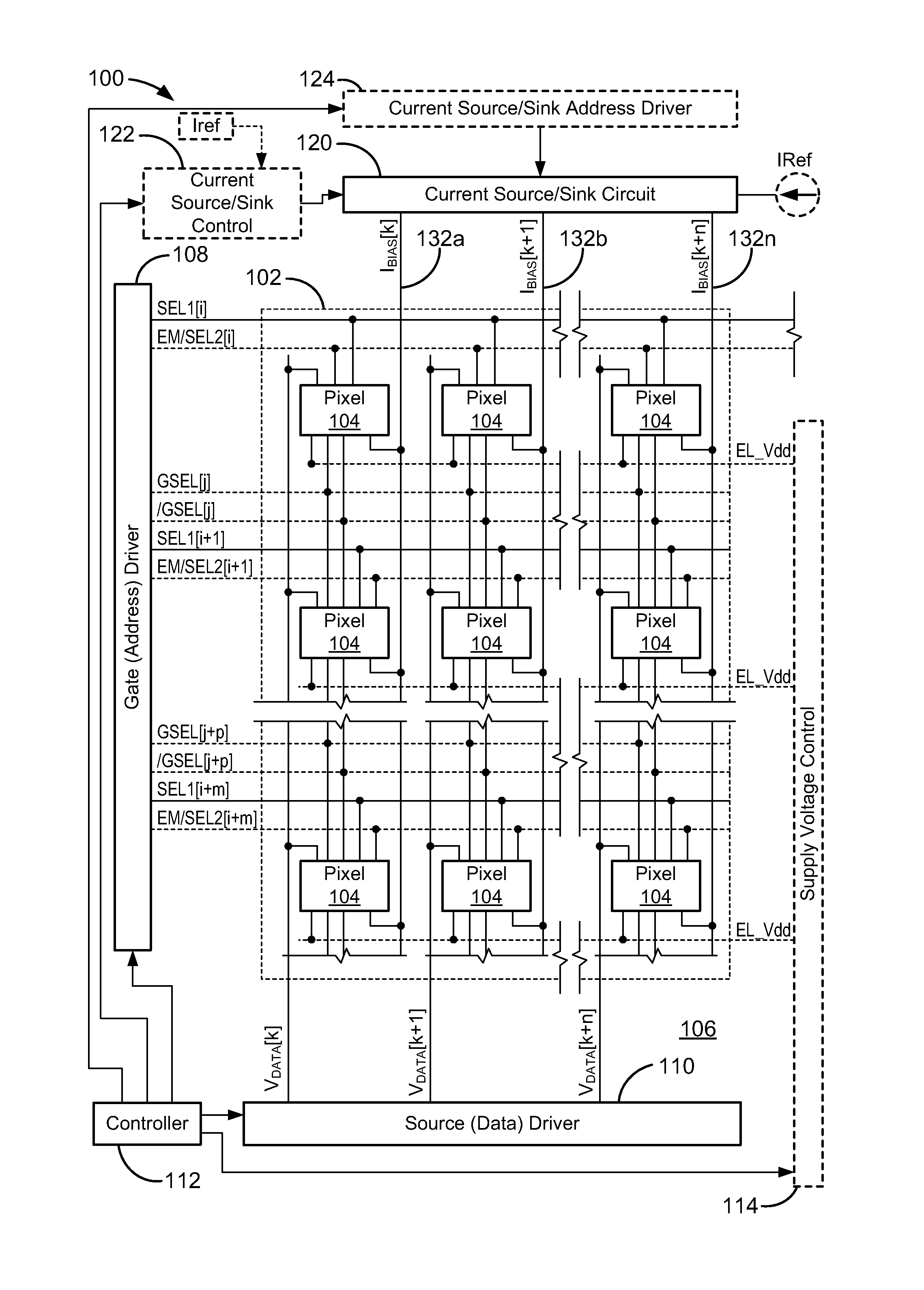
[0132]FIG. 1 is an electronic display system or panel 100 having an active matrix area or pixel array 102 in which an array of pixels 104 are arranged in a row and column configuration. For ease of illustration, only two rows and columns are shown. External to the active matrix area 102 is a peripheral area 106 where peripheral circuitry for driving and controlling the pixel area 102 are disposed. The peripheral circuitry includes a gate or address driver circuit 108, a source or data driver circuit 110, a controller 112, and an optional supply voltage (e.g., Vdd) control driver or circuit 114. The controller 112 controls the gate, source, and supply voltage drivers 108, 110, 114. The gate driver 108, under control of the controller 112, operates on address or select lines SEL[i], SEL[i+1], and so forth, one for each row of pixels 104 in the pixel array 102. In pixel sharing configurations described below, the gate or address driver circuit 108 can also optionally operate on global ...


PUM


Abstract

A technique for improving the spatial and/or temporal uniformity of a light-emitting display by providing a faster calibration of reference current sources and reducing the noise effect by improving the dynamic range, despite instability and non-uniformity of the transistor devices. A calibration circuit for a display panel having an active area having a plurality of light emitting devices arranged on a substrate, and a peripheral area of the display panel separate from the active area is provided. The calibration circuit includes a first row of calibration current source or sink circuits and a second row of calibration current source or sink circuits. A first calibration control line is configured to cause the first row of calibration current source or sink circuits to calibrate the display panel with a bias current while the second row of calibration current source or sink circuits is being calibrated by a reference current. A second calibration control line is configured to cause the second row of calibration current source or sink circuits to calibrate the display panel with the bias current while the first row of calibration current source or sink circuits is being calibrated by the reference current.

Description

CROSS-REFERENCE TO RELATED APPLICATION[0001]This application claims the benefit of Canadian Patent Application Serial No. 2,684,818, filed Nov. 12, 2009, entitled “Sharing Switch TFTS in Pixel Circuits,” Canadian Patent Application Serial No. 2,686,324, filed Dec. 6, 2009, entitled “Stable Current Source for System Integration to Display Substrate,” and Canadian Patent Application Serial No. 2,694,086, filed Feb. 17, 2010, entitled “Stable Fast Programming Scheme for Displays,” each of which is incorporated by reference in its entirety.COPYRIGHT[0002]A portion of the disclosure of this patent document contains material which is subject to copyright protection. The copyright owner has no objection to the facsimile reproduction by anyone of the patent disclosure, as it appears in the Patent and Trademark Office patent files or records, but otherwise reserves all copyright rights whatsoever.FIELD OF THE PRESENT DISCLOSURE[0003]The present disclosure generally relates to circuits and me...

Claims


Application Information

Patent Timeline
IPC IPC(8): G01R19/00H05B44/00
CPCG09G3/3283G09G3/3291G09G2300/0814G09G2300/0819G09G2300/0852G09G3/3225G09G2320/0233G09G2320/0693G09G2310/0218G09G2300/0465G09G2310/0262G09G5/18
Inventor CHAJI, GHOLAMREZANATHAN, AROKIA
Owner IGNIS INNOVATION
Why Eureka
Try Eureka