

Semiconductor memory which enables reliable data writing with low supply voltage by improving the conductance via access transistors during write operation
a technology of access transistor and data writing, which is applied in the field of single-port static random access memory, can solve the problems of inability to meet the conductance of writing operation of mos transistor pb>101/b>, inability to write operation reliable, and content stored in memory cells may become corrupted, etc., and achieve the effect of easy turning over
- Summary
- Abstract
- Description
- Claims
- Application Information
AI Technical Summary
Benefits of technology
Problems solved by technology
Method used
Image

Examples
first embodiment
[0073]FIG. 3 is a circuit diagram showing the memory cell M00 as a The memory cell M00 comprises a p-type MOS transistor P1 and an n-type MOS transistor N1 that are connected in series between a supply voltage VCC and a ground voltage VSS, and a p-type MOS transistor P2 and an n-type MOS transistor N2 that are connected in series between a supply voltage VCC and a ground voltage VSS. These MOS transistors N1, P1, N2 and P2 constitute a pair of inverters, which are cross-coupled, and a latch circuit, which maintains electrical potentials stable at junction T1 and at junction T2.
[0074]Furthermore, the memory cell M00 comprises an n-type MOS transistor N3 and an n-type MOS transistor N5 that are disposed between bit line BL and junction T1, which leads to p-type MOS transistor P1 and n-type MOS transistor N1. It further comprises an n-type MOS transistor N4 and an n-type MOS transistor N6 that are disposed between bit line XBL and junction T2, which leads to p-type MOS transistor P2 a...
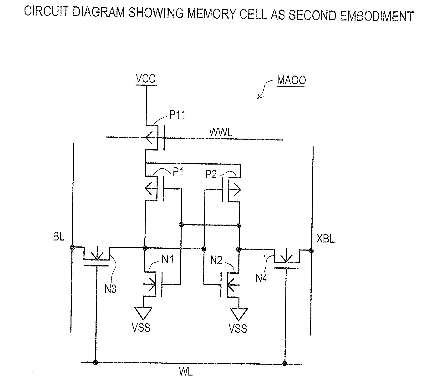
second embodiment
[0101]Therefore, the single port SRAM as a second embodiment retains the stored contents, which are represented by the electrical potentials at respective junctions T1 and T2 of the memory cell MA00, reliably even in a case where the margin for static noise on the threshold voltage Vth is relatively small because of a low supply voltage being applied. In addition, the SRAM can perform writing operation reliably.
[0102]Now, a single port SRAM as a third embodiment is explained. This SRAM has a general construction with a memory cell array similar to that of the first embodiment. The only difference is that the third embodiment comprises, instead of the write word line WWL, another write word line XWWL whose logical level is the reversal of that of the write word line WWL in the first embodiment. Therefore, only the part that relates to the write word line XWWL is explained here, so the same part as the first embodiment is not described here or is described in a simplified manner.
[0103...
third embodiment
[0111]Therefore, the single port SRAM as a third embodiment retains the stored contents, which are represented by the electrical potentials at respective junctions T1 and T2 of the memory cell MB00, reliably even in a case where the margin for static noise on the threshold voltage Vth is relatively small because of a low supply voltage being applied. In addition, the SRAM can perform writing operation reliably.
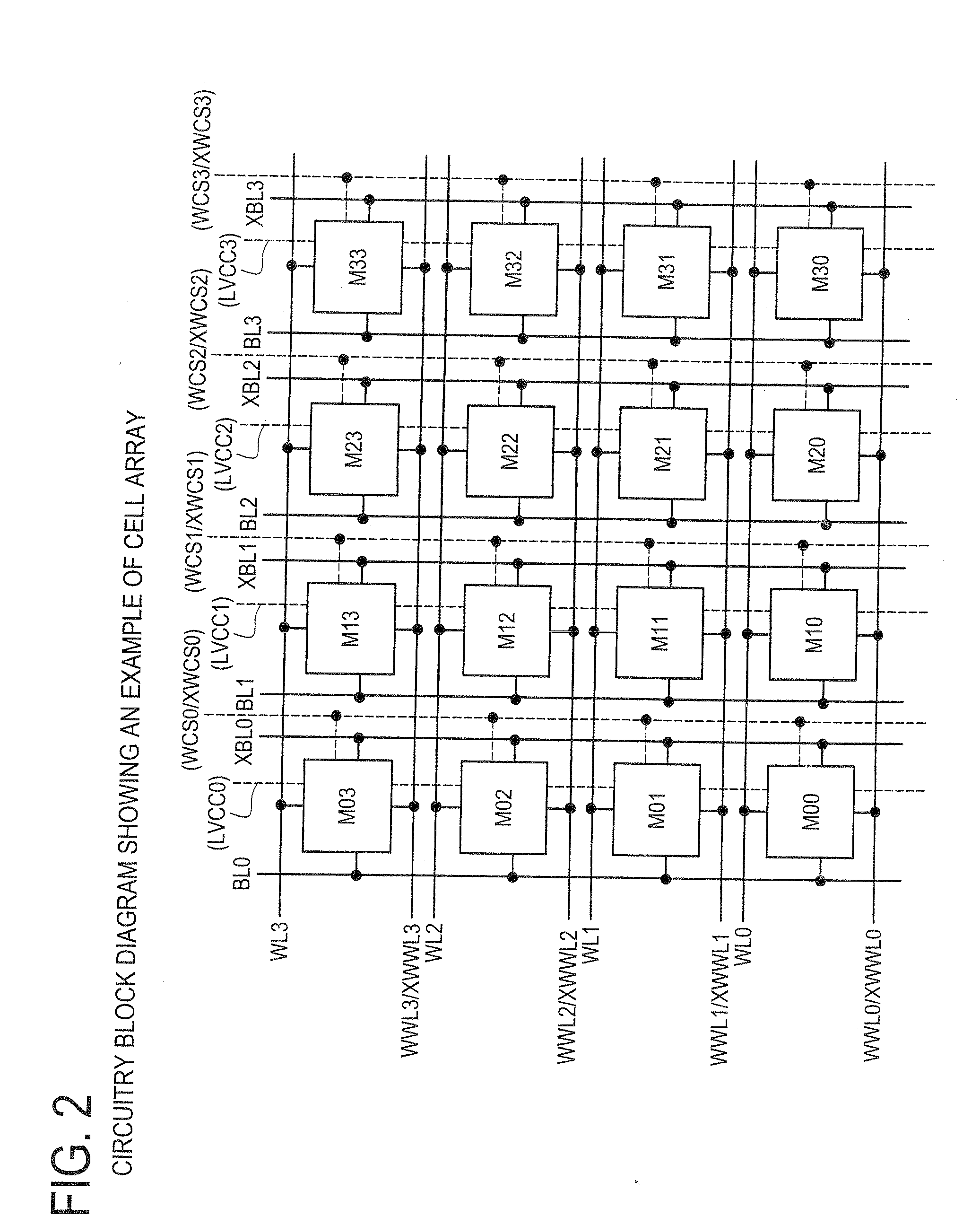
[0112]Now, a single port SRAM as a fourth embodiment is explained. This SRAM has a general construction with a memory cell array including a write word line XWWL, which is similar to that of the third embodiment. However, it is different from the third embodiment in that the memory cell array 1 includes a write column line WCS. Therefore, only the part that relates to the write column line WCS is explained, so the same part as the third embodiment is not described here or is described in a simplified manner.
[0113]At first, referring to FIG. 1, the column decoder 5 decodes lowe...
PUM
 Abstract
Description
Claims
Application Information