

Anti-fuse circuit and semiconductor memory device
a technology of anti-fuse circuit and semiconductor memory device, which is applied in logic circuits, digital storage, instruments, etc., can solve the problems of anti-fuse circuits and inability to program laser fuse, and achieve the effect of reliable writing
- Summary
- Abstract
- Description
- Claims
- Application Information
AI Technical Summary
Benefits of technology
Problems solved by technology
Method used
Image

Examples
example 1
[0032]FIG. 3 illustrates an anti-fuse writing circuit according to example 1, and a configuration and operations thereof will be hereinafter described. During a write operation, the anti-fuse writing circuit of FIG. 3 is supplied with five kinds of power supplies having power supply voltages VPPSVT, VDD1, VDD2, VSS, and VBBSVT in the order of highest to lowest. Preferably, VPPSVT is 6.5 V, VDD1; 1.8 V, VDD2; 1.2 V, VSS; 0 V, and VBBSVT; −3.5 V.
[0033]A STORE signal is a write data signal in the VDD2 system sent to an anti-fuse circuit 7. When the STORE signal is at a low level during a write operation, a current flows through an anti-fuse element Fuse, which is then brought to be in an on state. When the STORE signal is at a high level, since no current flows through the anti-fuse element Fuse, the anti-fuse element Fuse is maintained in a high impedance state. A level shifter LS1 is supplied with the power supplies VDD1, VDD2, and VSS and increases the STORE signal, which is a logic...
example 2
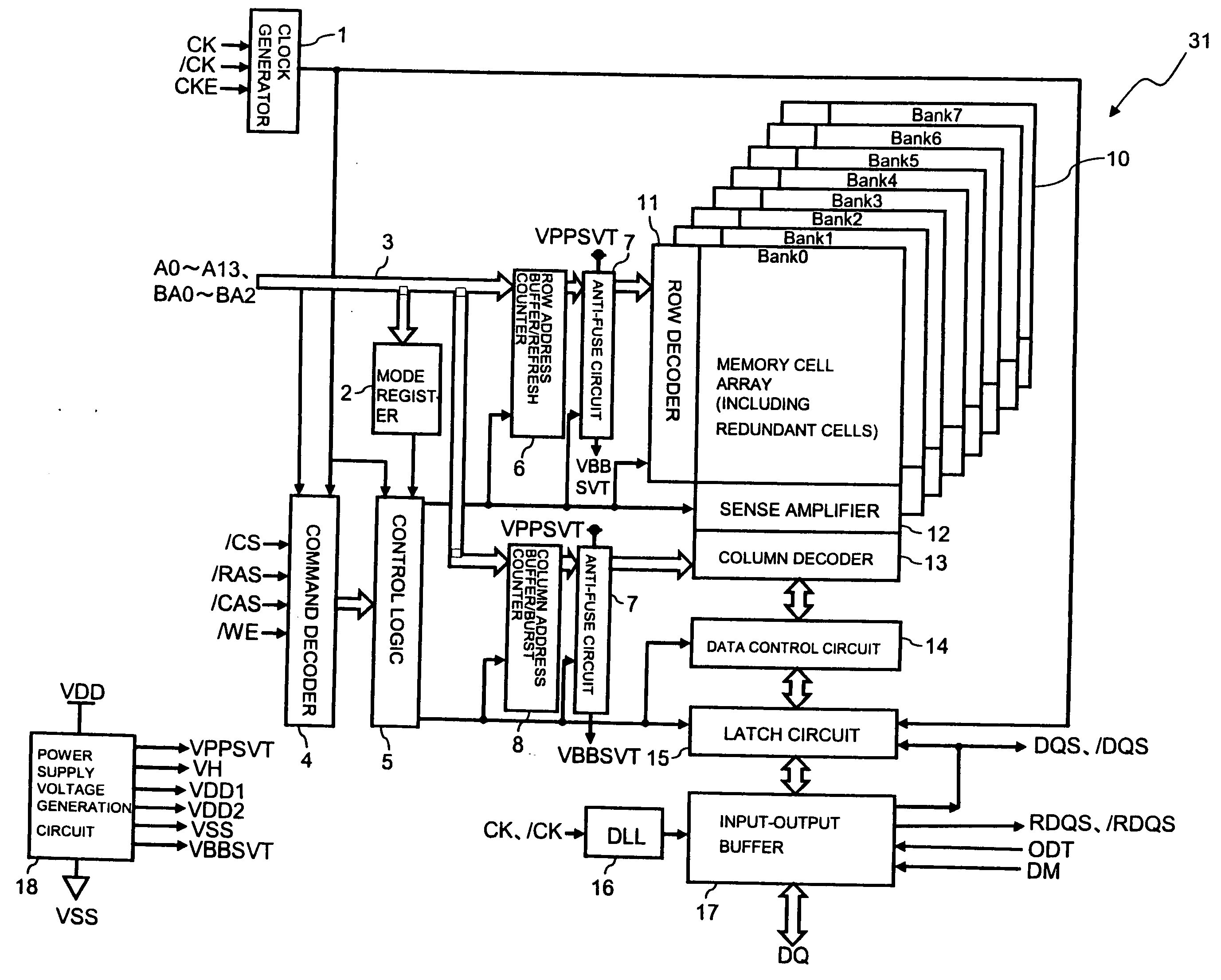
[0041]Next, an example where an anti-fuse circuit is used in a semiconductor memory device such as a dynamic random access memory (DRAM) will be described. FIG. 5 is a block diagram illustrating an overall configuration of a semiconductor memory device according to example 2. In FIG. 5, a semiconductor memory device 31 is a synchronous DRAM. An overall configuration of the semiconductor memory device 31 of FIG. 5 will be hereinafter described. A clock generator 1 receives clock signals CK and / CK and a clock enable signal CKE from the outside and supplies these clocks to the entire semiconductor memory device 31. An address bus 3 receives address signals A0 to A13 and bank address signals BA0 to BA2 from the outside and sends these signals to a mode register 2, a row address buffer / refresh counter 6, and a column address buffer / burst counter 8. The mode register 2 receives address data from the address bus 3 and sets an internal operation mode. A command decoder 4 receives a chip se...
example 3
[0044]FIG. 6 illustrates power supply channels of a semiconductor memory device according to example 3. Example 3 is an example where the power supply voltage generation circuit 18 in example 2 is separately arranged in portions of the semiconductor memory device 31. FIG. 6 only illustrates power supply channels of the VDD2, VDD1, VH, and VPPSVT systems. In FIG. 6, both the power supplies VDD1 and VDD2 are supplied from the outside via external terminals VDD1 and VDD2. However, this is merely an example; only one of the power supplies VDD1 and VDD2 may be supplied from the outside, and the other power supply may be generated in the semiconductor memory device 31. In example 3, as in examples 1 and 2, the voltages VDD2, VDD1, VH, and VPPSVT are preferably 1.2 V, 1.8 V, 2.7 V, and 6.5 V, respectively.
[0045]The power supply VDD1 supplied from the external power supply terminal VDD1 is supplied to a memory-cell voltage-boost circuit 20 and a switch SW1. The memory-cell voltage-boost cir...
PUM
 Abstract
Description
Claims
Application Information