
Method and System for Providing Secondary Power Pins in Integrated Circuit Design

a technology of integrated circuits and secondary power pins, applied in the direction of instruments, computing, electric digital data processing, etc., can solve the problems of gate delay increase and signal delay

Active Publication Date: 2011-05-12
GLOBALFOUNDRIES US INC
View PDF12 Cites 25 Cited by
  • Summary
  • Abstract
  • Description
  • Claims
  • Application Information

AI Technical Summary

Problems solved by technology

An important aspect of IC design consists in ensuring signal integrity: If the wire resistance and / or cell current of some cells within the IC exceeds a predetermined limit, voltage drops (aka IR drops) may occur, causing an increase of gate and signal delays and—in the worst case—switching failures of the integrated circuit.

Method used


Image

  • Method and System for Providing Secondary Power Pins in Integrated Circuit Design
  • Method and System for Providing Secondary Power Pins in Integrated Circuit Design
  • Method and System for Providing Secondary Power Pins in Integrated Circuit Design

Examples


Embodiment Construction

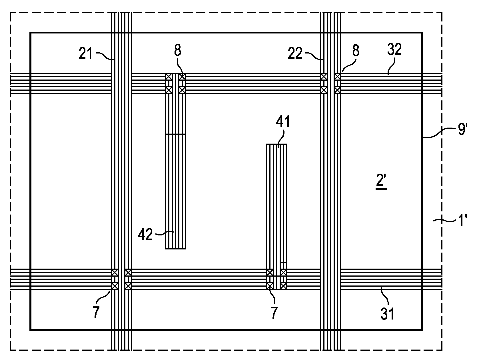
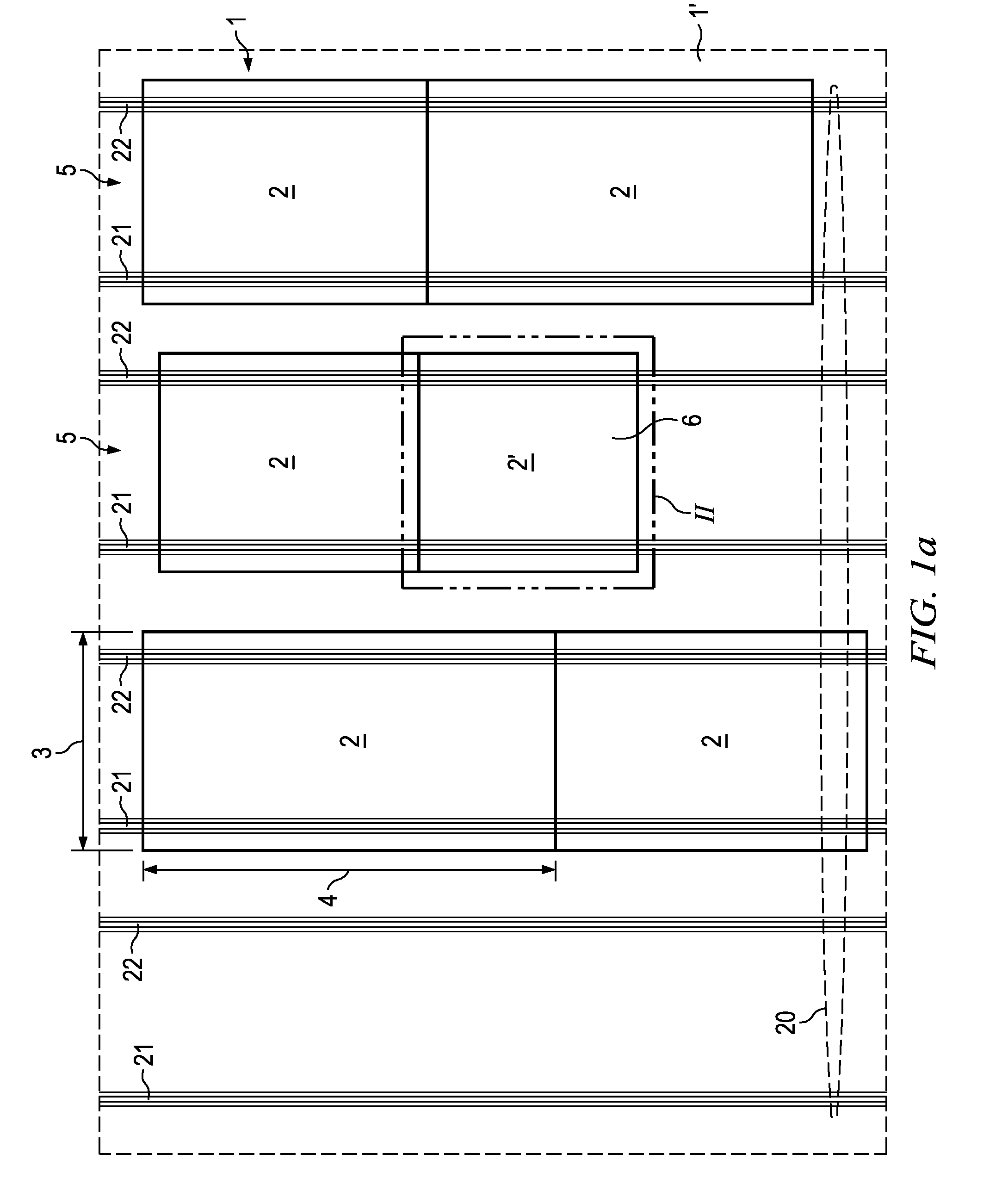
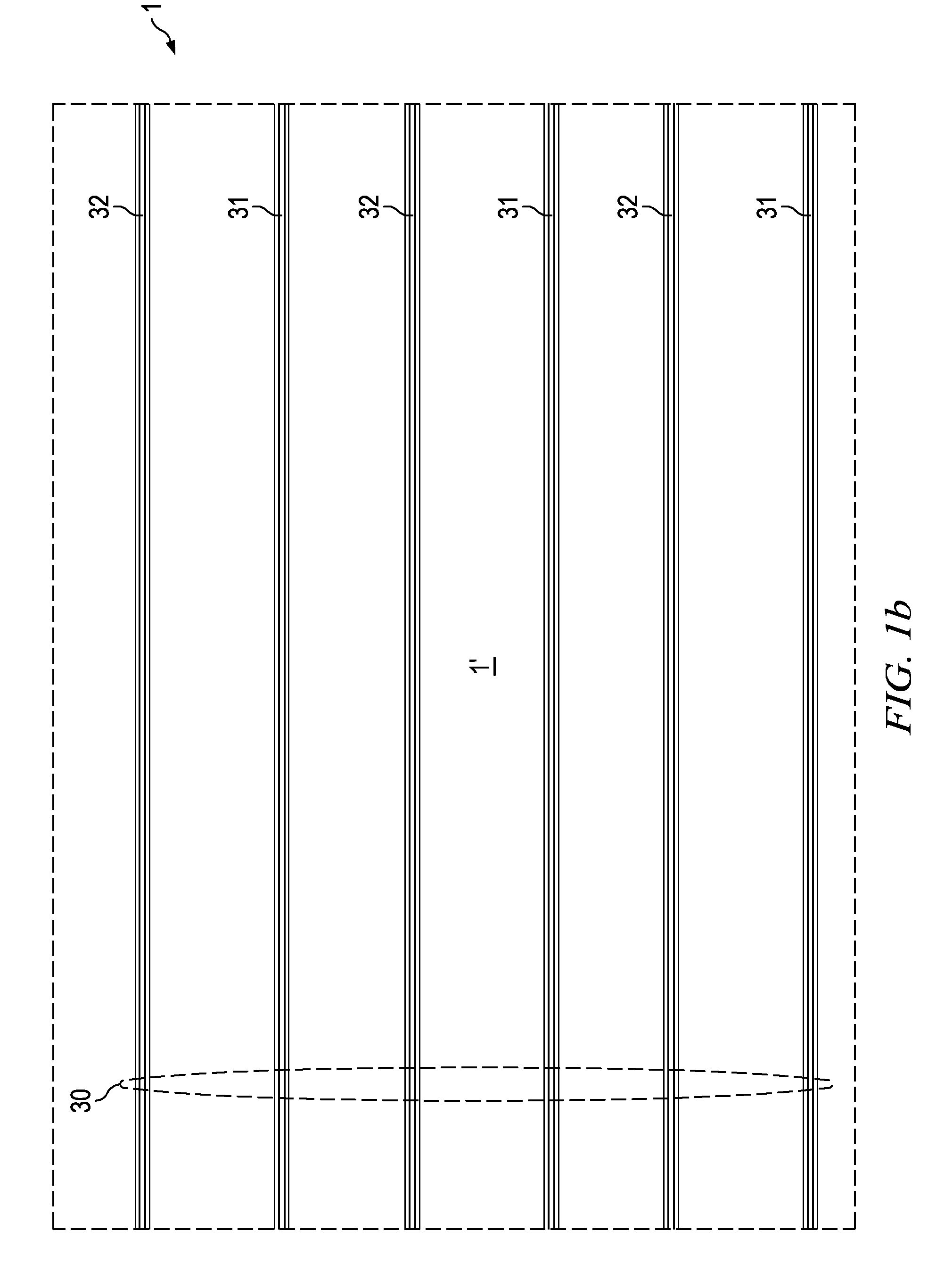
[0030]Integrated circuits (ICs) comprise a multitude of electronic and circuit components which are electrically connected to each other using metal interconnects arranged in planar layers (so-called “metal layers” M1, M2, M3, . . . ). Up to ten (or even more) of these metal layers may be stacked on top of each other. Each metal layer comprises a primary power wiring network which is formed by a set of electronically conducting stripes supplying power (vdd) or ground (gnd). Voltage for powering the primary power wiring network is supplied by an external power supply source; typically, ring structures at the edges of the IC form the backbone of the power distribution system. In order to facilitate signal routing and power distribution, the primary power wiring network is typically implemented by a row pattern of parallel alternating power (vdd) and ground (gnd) stripes aligned in a preferred wiring direction. The preferred wiring directions of successive metal layers are perpendicula...


PUM


Abstract

An integrated circuit (IC) design with multiple metal layers containing cells requiring secondary power supply. After placing the cells and stripes of a primary power / ground grid in metal layers of the IC design, specific cells are provided with secondary power stripes in a first metal layer. The secondary power stripes are designed in such a way that each secondary power / ground stripe exhibits a full overlap with a stripe of a corresponding primary power / ground grid in a different metal layer. Subsequently, signals from the IC design are routed, and power vias between the primary power / ground grid stripes and the secondary power / ground stripes are generated.

Description

BACKGROUND[0001]1. Field[0002]The invention relates generally to the design of semiconductor integrated circuits (ICs). More specifically, the invention relates to a method for ensuring signal integrity in integrated circuits with multiple metal layers, by introducing a secondary power grid for providing additional supply voltage to logic cells with high power consumption within the design.[0003]2. Description of the Related Art[0004]An integrated circuit (IC) is a device which includes a plurality of electronic components (e.g. transistors, resistors, diodes etc.). These components are interconnected to form multiple circuit components (gates, cells, memory units etc.) on the IC. Modern very large scale integration (VLSI) integrated circuits are typically made up of a layer structure with multiple layers of wiring (called “metal layers”) that interconnect its electronic and circuit components. Each metal layer typically has a preferred wiring direction, and the preferred direction ...

Claims


Application Information

Patent Timeline
IPC IPC(8): G06F17/50
CPCG06F17/5077G06F30/394
Inventor KEINERT, JOACHIMLAMB, DOUGLASS T.OSLER, PETER J.
Owner GLOBALFOUNDRIES US INC
Learn More