Method of manufacturing semiconductor integrated circuit device

a semiconductor integrated circuit and integrated circuit technology, applied in semiconductor devices, electrical devices, instruments, etc., can solve problems such as device damage, pattern deformation,

Inactive Publication Date: 2011-06-02
RENESAS ELECTRONICS CORP
View PDF6 Cites 25 Cited by
  • Summary
  • Abstract
  • Description
  • Claims
  • Application Information

AI Technical Summary

Benefits of technology

[0022]That is, in the exposure to light of a memory cell array or the like of a semiconductor memory or the like, when the group of unit openings for etching the STI trench regions in which the unit openings for etching the STI trench regions each having a horizontally elongated substantially rectangular shape are arranged in rows and columns are transferred by the exposure onto a negative resist film, the multiple exposure is appropriately used which includes the first exposure step using the first optical mask having the group of first linear openings extending in the column direction and the second exposure step using the second optical mask having the group of second linear openings extending in the row direction. Therefore, it is possible to avoid a proximity effect at an end portion of the rectangular shape.

Problems solved by technology

There is a concern that such pattern deformation may affect device parameters such as the gate width of a memory gate longitudinally traversing the vicinity of the end portion.

Method used


Image

  • Method of manufacturing semiconductor integrated circuit device
  • Method of manufacturing semiconductor integrated circuit device
  • Method of manufacturing semiconductor integrated circuit device

Examples


Embodiment Construction

Explanation of Description Form, Basic Terminology, and use Thereof in Present Invention

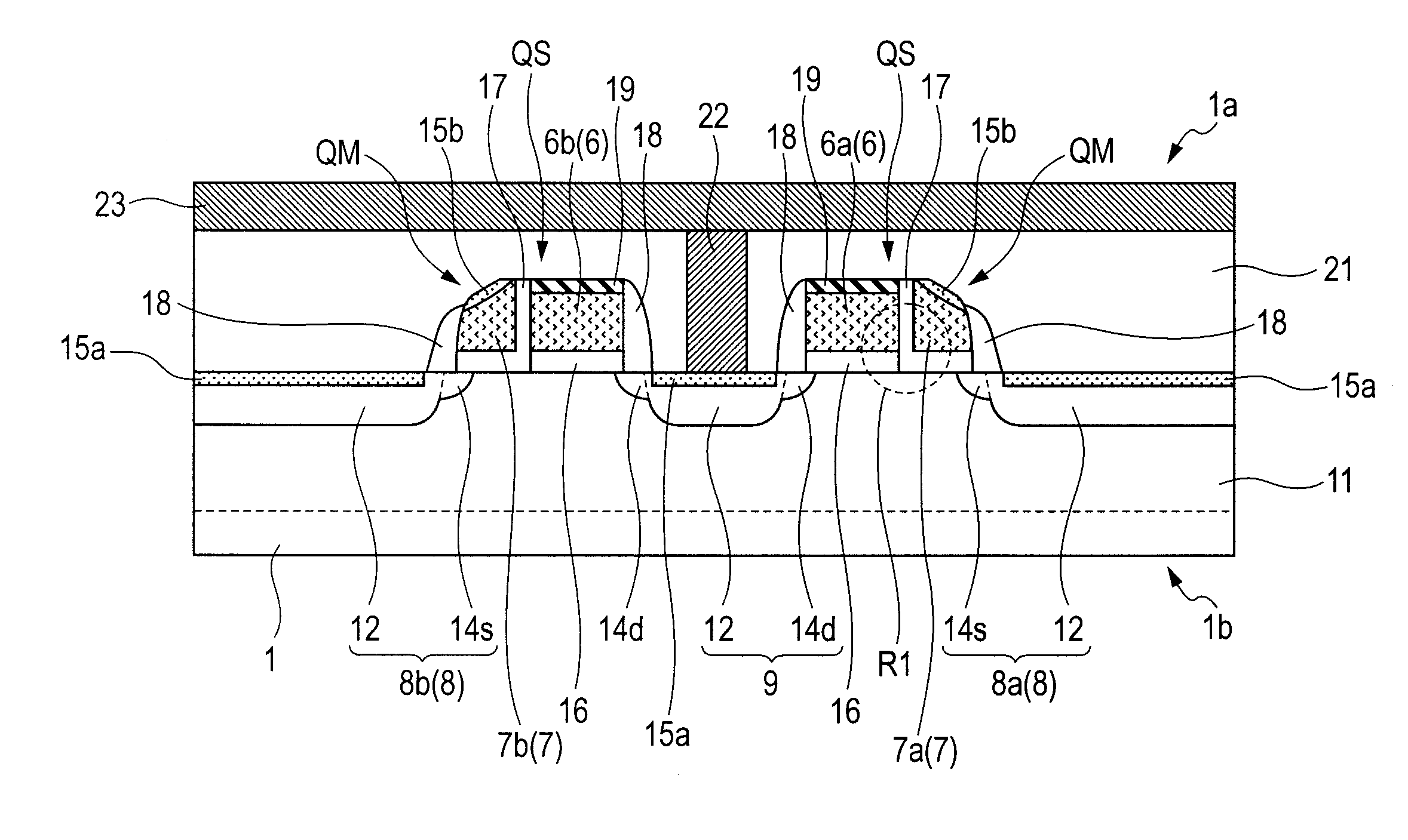
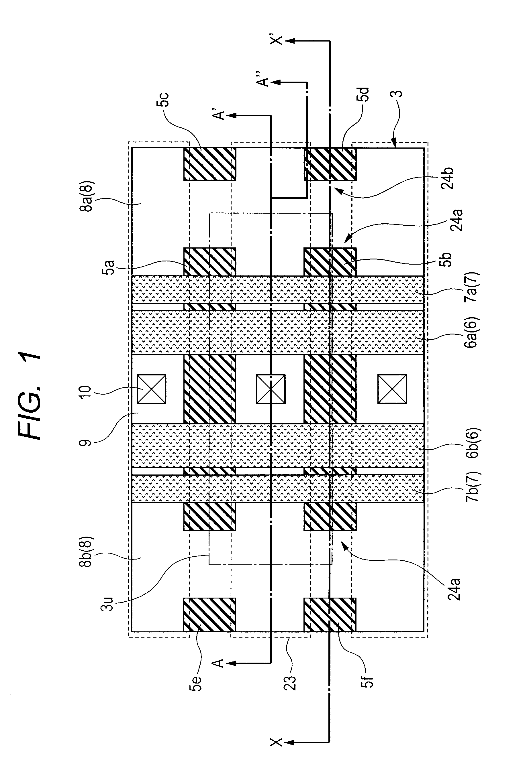
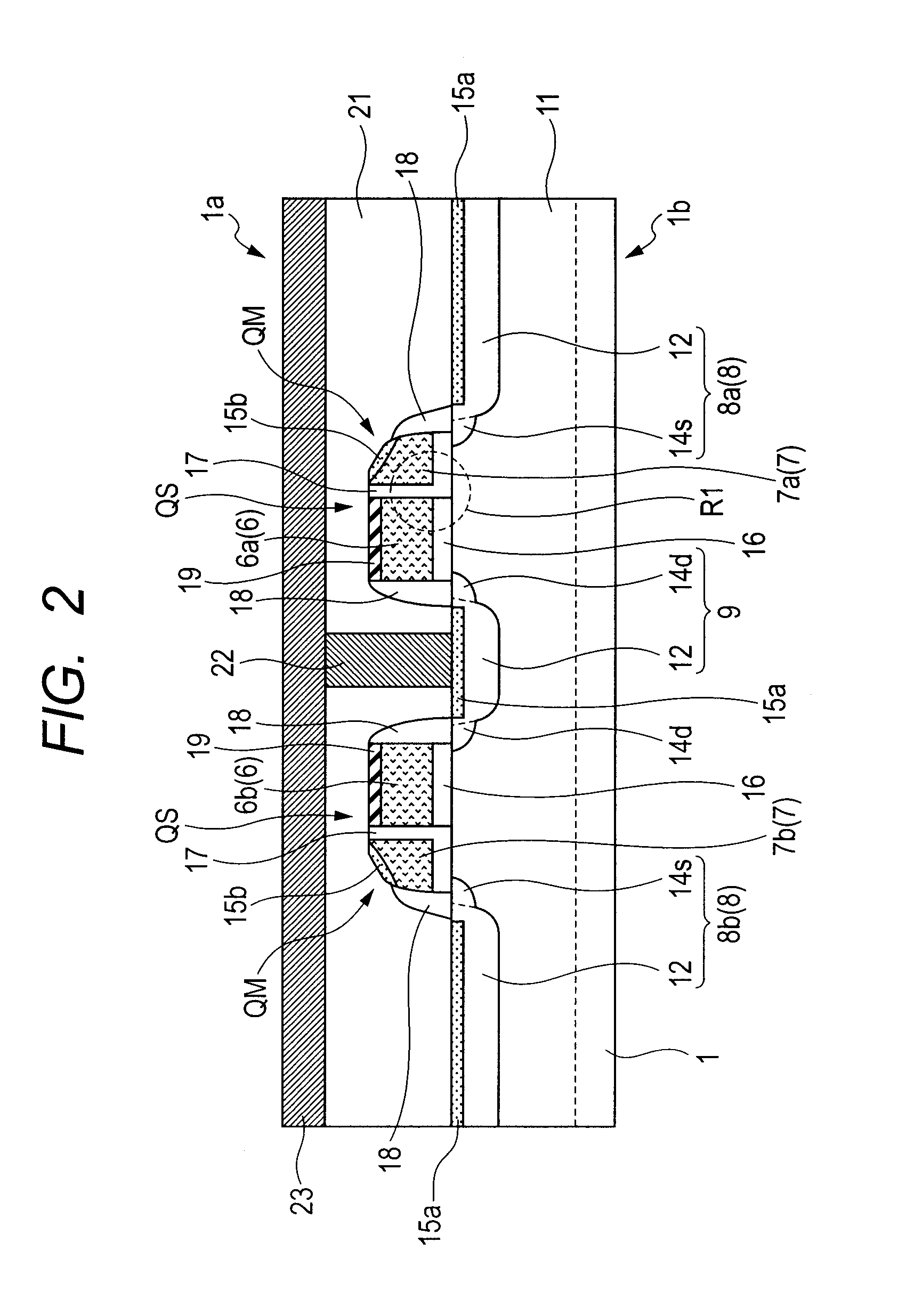
[0082]1. In the present invention, if necessary for the sake of convenience, the description of an embodiment may be such that the embodiment is divided into a plurality of sections in the description thereof. However, they are by no means independent of or distinct from each other unless particularly explicitly described otherwise, and one of the individual parts of a single example is details, variations, and so forth of part or the whole of the others. In principle, a repeated description of like parts will be omitted. Each constituent element in the embodiment is not indispensable unless particularly explicitly described otherwise, unless the constituent element is theoretically limited to a specific number, or unless it is obvious from the context that the constituent element is indispensable.

[0083]Also in the present invention, when a “semiconductor device” or semiconductor integrated circu...


PUM


Abstract

In the present invention, in the exposure to light of a memory cell array or the like of a semiconductor memory or the like, when a group of unit openings for etching the STI trench regions in which the unit openings for etching the STI trench regions each having a rectangular shape are arranged in rows and columns are transferred by the exposure onto a negative resist film, multiple exposure is appropriately used which includes a first exposure step using a first optical mask having a group of first linear openings extending in a column direction and a second exposure step using a second optical mask having a group of second linear openings extending in a row direction.

Description

CROSS-REFERENCE TO RELATED APPLICATIONS [0001]The disclosure of Japanese Patent Application No. 2009-273241 filed on Dec. 1, 2009 including the specification, drawings and abstract is incorporated herein by reference in its entirety.BACKGROUND OF THE INVENTION[0002]The present invention relates to a technology which is effective when applied to a lithography technique in a method of manufacturing a semiconductor integrated circuit device (or semiconductor device).[0003]In Japanese Unexamined Patent Publication No. Hei 5(1993)-326358 (Patent Document 1), a technology is disclosed in which one negative resist film is exposed to light twice using two masks having respective band-like light shielding portions orthogonal to each other so as to prevent the shape of a corner portion of a contact hole from being rounded.[0004]In Japanese Unexamined Patent Publication No. Hei 9(1997)-289153 (Patent Document 2), a technology is disclosed in which, in photolithographic processing using a polyc...

Claims


Application Information

Patent Timeline
Patent Type & Authority Applications(United States)
IPC IPC(8): H01L21/762
CPCG11C16/0425G11C16/0433H01L21/76229H01L21/823425H01L29/792H01L21/823468H01L27/11565H01L27/11573H01L21/823456H10B43/10H10B43/40
Inventor FUNAYAMA, KOTACHAKIHARA, HIRAKU
Owner RENESAS ELECTRONICS CORP
Why Eureka
Try Eureka