Via Structure Integrated in Electronic Substrate

a technology of electronic substrates and vias, applied in the direction of resistive material coating, coupling device connections, metallic pattern materials, etc., can solve the problems of eddy current loss in the substrate, negative impact on the operation of the electrical package, and eddy current loss still remains a problem, so as to and reduce electrical or magnetic fields

Active Publication Date: 2011-06-16
QUALCOMM INC
View PDF26 Cites 30 Cited by
  • Summary
  • Abstract
  • Description
  • Claims
  • Application Information

AI Technical Summary

Benefits of technology

In a different embodiment, a method of reducing electrical or magnetic fields in an electronic device is provided. The method includes forming a first conductive layer in a substrate and surrounding the first conductive layer with an insulating layer. The insulating layer is surrounded by a second conductive layer. The method includes passing a first signal of a complementary pair through the first conductive layer and a second signal of the complementary pair through the second conductive layer such that the second conductive layer is adapted to reduce electrical or magnetic fields produced by the first signal passing through the first conductive layer. In one form thereof, the method includes coupling the second conductive layer to a first potential. In another form thereof, the method includes coupling the second conductive layer to a salicide material. The method can also include forming another insulating layer that surrounds the second conductive layer.
In another exemplary embodiment, a via structure for reducing electrical or magnetic fields in an electronic device is provided. The via structure includes a first conductive means for conducting a first signal of a complementary pair in a substrate and a second conductive means for conducting a second signal of the complementary pair in the substrate. The via structure also includes an insulating means for insulating the first conductive means from the second conductive means. The first signal and second signal comprise substantially opposite polarities.

Problems solved by technology

For example, mutual inductance between nearby TSVs can cause cross-talk, which in some instances can negatively impact the operation of the electrical package.
Another design challenge associated with a TSV is the creation of eddy current losses in the substrate.
However, eddy current losses still remain a problem.

Method used


Image

  • Via Structure Integrated in Electronic Substrate
  • Via Structure Integrated in Electronic Substrate
  • Via Structure Integrated in Electronic Substrate

Examples


Embodiment Construction

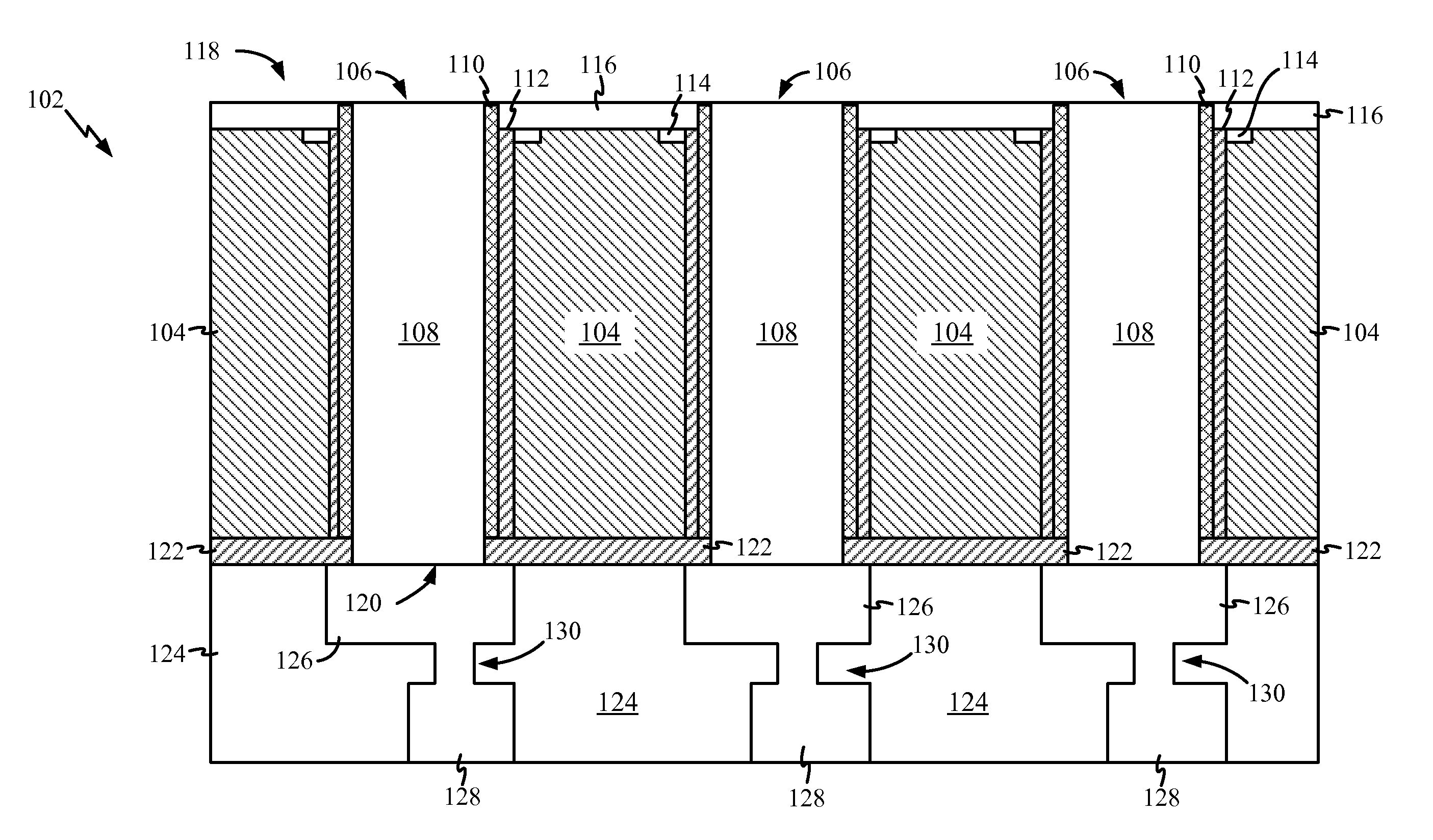
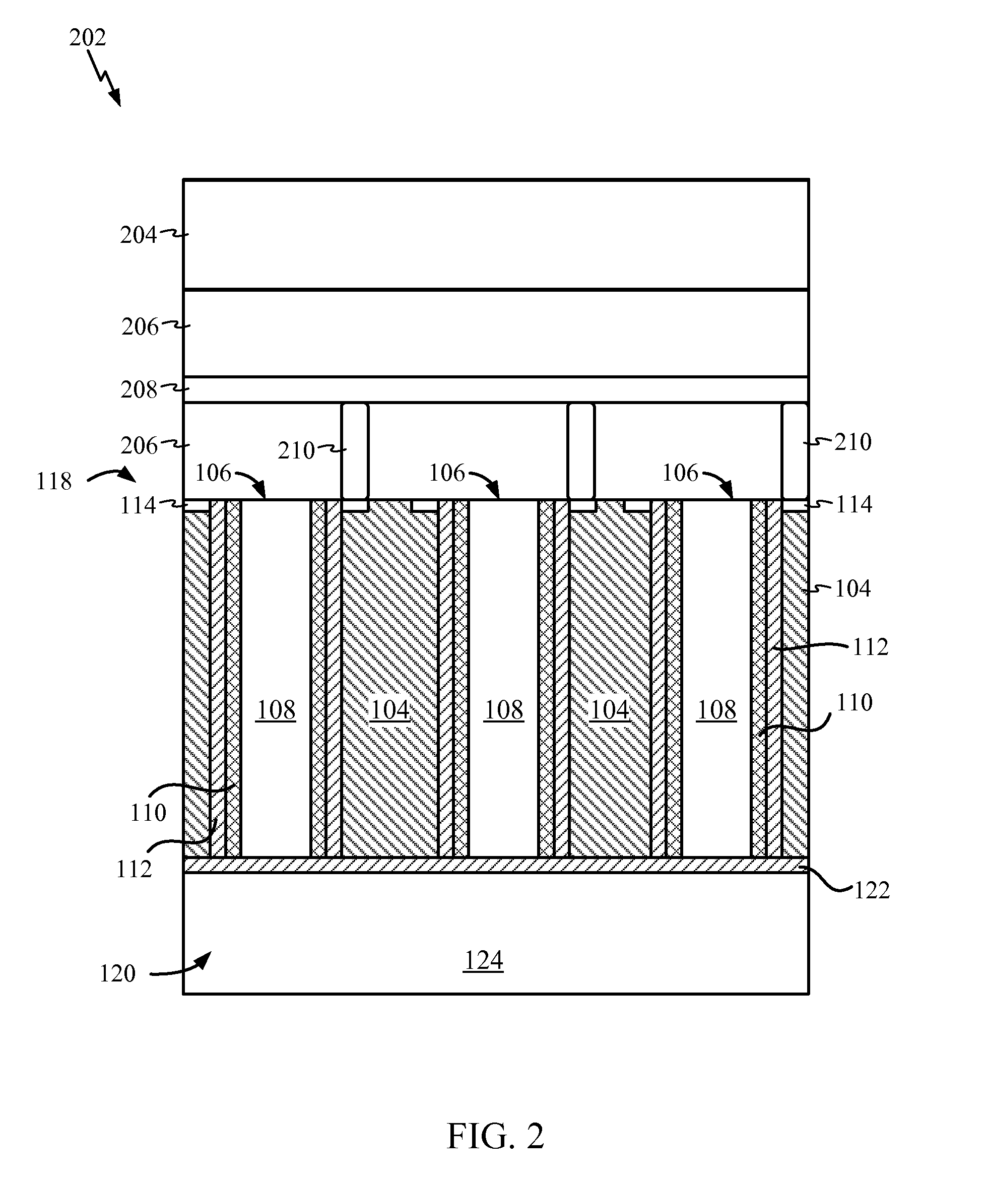
Referring to the embodiment shown in FIG. 1, an electronic structure 102 is provided. The electronic structure 102 includes a substrate 104 with a plurality of TSVs 106 disposed therein. Although not shown, in various embodiments the plurality of TSVs 106 can be arranged in the substrate as an array or cluster of TSVs. The substrate 104 can be made of materials such as silicon, silicon carbide, silicon dioxide, silicon nitride, or any other substrate material known to the skilled artisan. The substrate 104 can be a multilayer substrate such as a buildup or laminate multilayer printed circuit board, or a buildup or laminate package substrate.

Each of the plurality of TSVs 106 includes a conductive layer 108, an insulating or dielectric layer 110, and a shield layer 112 which can be in contact with the substrate 104. The insulating or dielectric layer 110 is positioned between the conductive layer 108 and shield layer 112. The insulating or dielectric material 110 can be made of an oxi...


PUM

PropertyMeasurementUnit
thicknessaaaaaaaaaa
mutual inductanceaaaaaaaaaa
heightaaaaaaaaaa

Abstract

A system of via structures disposed in a substrate. The system includes a first via structure that comprises an outer conductive layer, an inner insulating layer, and an inner conductive layer disposed in the substrate. The outer conductive layer separates the inner insulating layer and the substrate and the inner insulating layer separates the inner conductive layer and the outer conductive layer. A first signal of a first complementary pair passes through the inner conductive layer and a second signal of the first complementary pair passes through the outer conductive layer. In different embodiments, a method of forming a via structure in an electronic substrate is provided.

Description

FIELD OF DISCLOSUREThis disclosure relates generally to electronic substrates, and in particular to an electronic substrate having a via structure.BACKGROUNDRecent developments in packaging technologies for integrated circuits have introduced a through-silicon via (TSV) which is a vertical electrical coupling passing through a silicon wafer or die. TSV is important for creating 3D electrical packages such that conductive layers can be stacked on top of one another and a signal can pass between the conductive layers by utilizing the TSV.In a conventional packaging design, there can be an array or cluster of TSVs for passing signals between different conductive layers. Besides occupying space in the substrate, the TSVs can also affect the functionality of adjacent or nearby TSVs. For example, mutual inductance between nearby TSVs can cause cross-talk, which in some instances can negatively impact the operation of the electrical package. To reduce the effects of mutual inductance, the ...

Claims


Application Information

Patent Timeline
Patent Type & Authority Applications(United States)
IPC IPC(8): H05K1/09B05D5/12H01R13/648H01R43/00
CPCH01L23/14Y10T29/49117H01L23/552H01L23/645H01L23/66H01L2223/6616H01L2223/6622H01L2223/6638H01L2924/3011H05K1/0222H05K1/0245H05K3/4602H05K3/4644H05K2201/09809H01L2924/0002H01L23/49827H01L2924/00H01L21/76898H01L23/481H01L23/48H01L23/522
Inventor LI, XIAZHAO, WEICAO, YUGU, SHIQUNKANG, SEUNG H.KING, MING-CHU
Owner QUALCOMM INC
Why Eureka
Try Eureka