High performance source for electron beam projection lithography

a lithography and electron beam technology, applied in the field of electron beam projection lithography tools, can solve the problems of insufficient throughput of probe-forming tools to support the production quantity of integrated circuits at the present state of the art, complex design, and difficulty in adjustmen

Inactive Publication Date: 2003-05-08
NIKON CORP
View PDF0 Cites 3 Cited by
  • Summary
  • Abstract
  • Description
  • Claims
  • Application Information

AI Technical Summary

Problems solved by technology

However, the graphic pattern complexity increases with integration density.
Therefore, while probe-forming electron beam exposure tools are often used at the present time for custom chips and application specific integrated circuits (ASICS) which are usually manufactured in limited quantities, probe-forming tools have insufficient throughput to support production quantities of integrated circuits at the present state of the art.
Unfortunately, an electron beam projection tool must deliver images at the target or wafer plane of extremely good fidelity to the reticle pattern and are thus of substantial complexity in design and difficult to adjust in order to obtain optimum or even adequate performance.
Minimiz

Method used


Image

  • High performance source for electron beam projection lithography
  • High performance source for electron beam projection lithography
  • High performance source for electron beam projection lithography

Examples


first embodiment

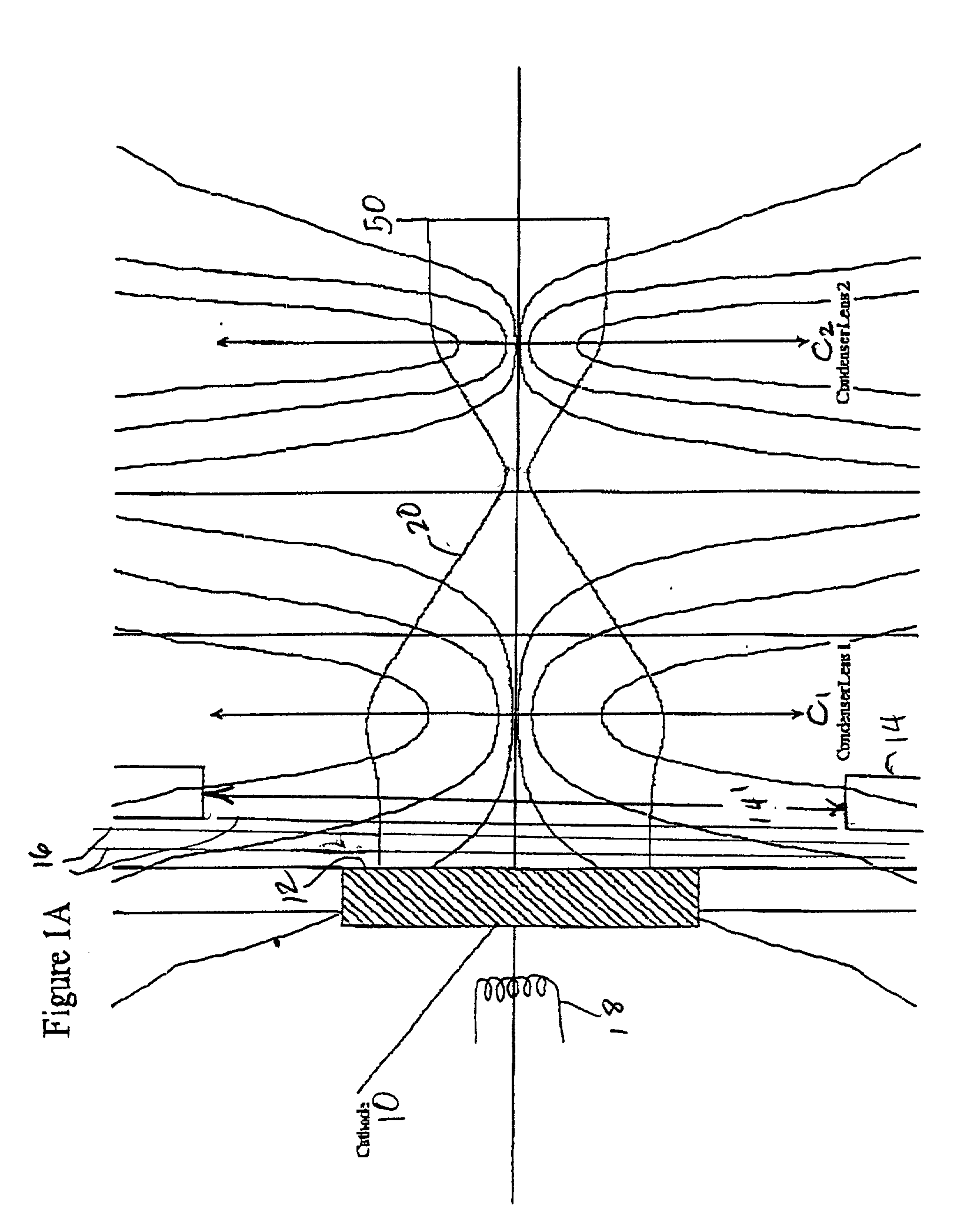
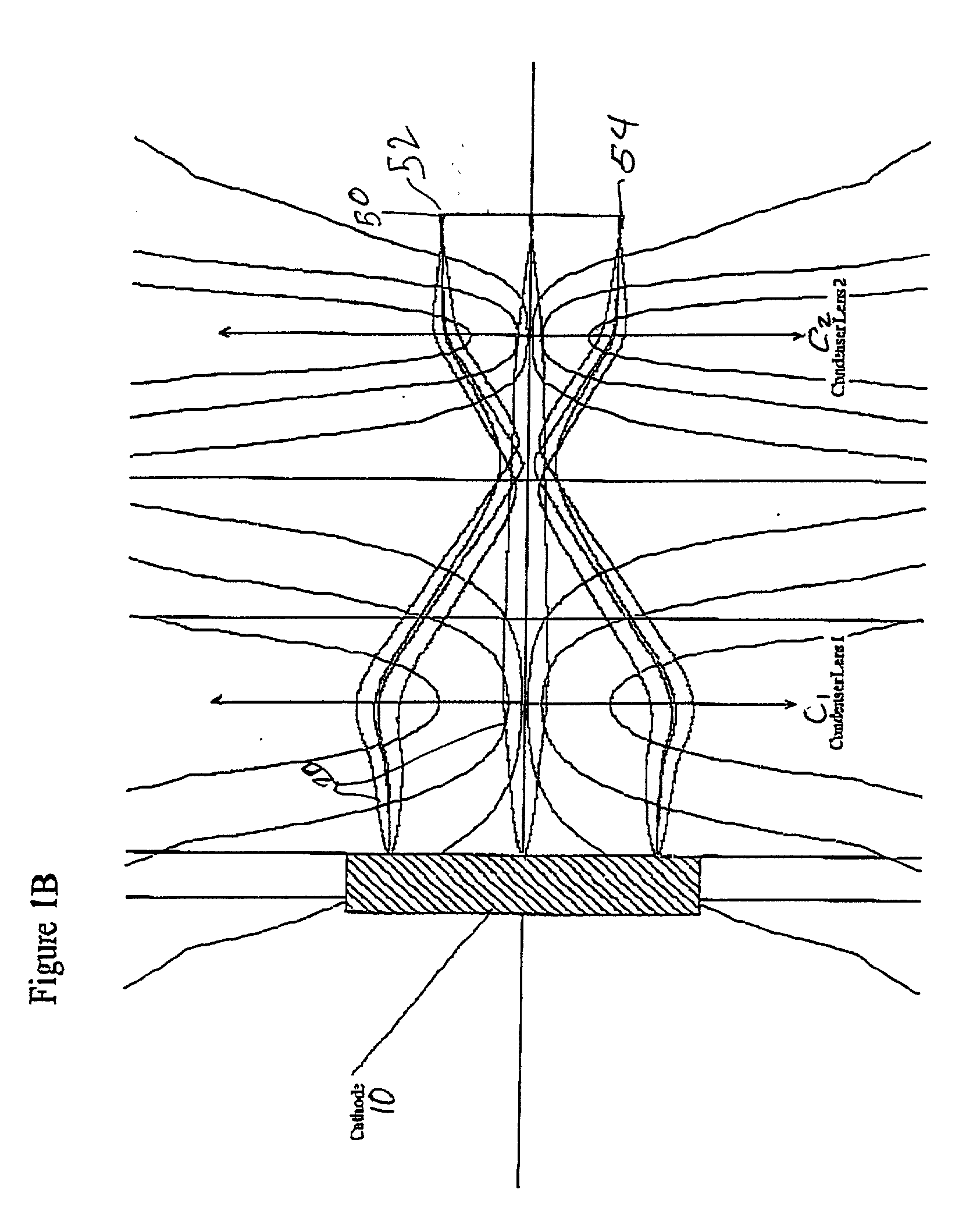
[0037] Referring now to FIG. 2A, the invention will be discussed. The positions of the electron-optical elements as depicted in FIG. 2A are essentially the same as in FIG. 1A except that the surface 12 of cathode 10 is displaced from the anode 14 and condenser C1 by a moderate amount of, for example, 40 mm. It has been found that the result is already substantial, as shown in FIG. 2B, as electrons from the emitter points far off the axis closely approach the axis, thus reducing the cross-over in size to almost its theoretical minimum.

[0038] It should be understood that the excitations of both condenser lenses C1 and C2 must be readjusted to re-establish the proper imaging conditions required by the entire projection system. The trajectories illustrated in FIG. 2A (and 3A) do not show the trajectories after such readjustment but are intended to illustrate the important effect of the invention on the crossover which serves as the illumination source for the remainder of the system.

second embodiment

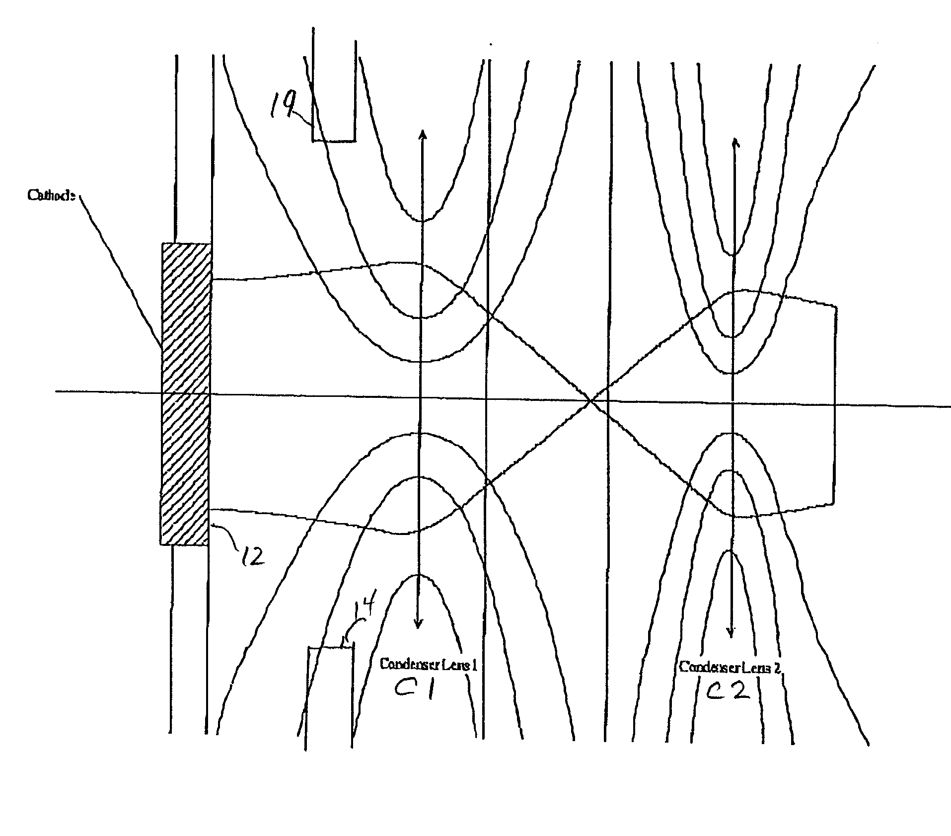
[0039] the invention will now be explained in connection with FIG. 3A. FIG. 3A is the same as FIG. 1A except that an additional thin magnetic lens, referred to as a bucking lens, C.sub.B is interposed between first condenser lens C1 and the cathode (and preferably within or preceding the anode), and the improved electron trajectories achieved thereby are shown. This lens is preferably driven proportionally and with the opposite polarity to first condenser lens C1 such that the magnetic field at the surface 12 of cathode 10 is reduced to zero (e.g. fully counterbalancing the field of lens C1).

[0040] Therefore, lens C.sub.B fully shields the cathode from the field of the first condenser lens C1 and effectively eliminates the magnetic field which can impart angular momentum to the electrons until they have been substantially accelerated by the electrostatic field between the cathode 12 and anode 14 and cannot be perturbed as readily as is possible at lower velocities and energies, as c...


PUM


Abstract

The presence of magnetic fields from lenses and other (e.g. parasitic) sources at locations in a charged particle beam system such as the charged particle emitter, where the particles have little or no kinetic energy, creates disturbances of the charged particle trajectories, generating undesired angular momentum and resulting in excessive aberrations and associated adverse effects on system performance. Solutions are provided by suppression of these magnetic fields, by relocating the charged particle emitter away from the field source and/or counterbalancing the field with a bucking field. In addition, residual irrepressible field asymmetries are compensated by a suitable element such as a stigmator located at the correct location in the beam path, permitted by relocation of the charged particle emitter.

Description

[0001] 1. Field of the Invention[0002] The present invention generally relates to charged particle beam tools and, more particularly, to electron beam projection lithography tools having electron (charged particle) emitter or cathode of large dimensions.[0003] 2. Description of the Prior Art[0004] Charged particle beam tools are known for numerous applications such as electron beam microscopy. Numerous applications have also been developed in the semiconductor device manufacturing industry such as for impurity implantation and lithographic exposures of patterns having feature sizes with dimensions smaller than can be resolved using electromagnetic radiation and the manufacture of x-ray lithography masks which must be formed at the same minimum feature size as the exposure to be made. In this regard, reduced feature sizes and increased integration density in integrated circuits provides increased performance and functionality as well as providing increases in manufacturing economy.[0...

Claims


Application Information

Patent Timeline
IPC IPC(8): G21K1/00G21K5/04H01J37/07H01J37/141H01J37/153H01J37/305H01L21/027
CPCH01J37/07
Inventor GOLLADAY, STEVEN D.GORDON, MICHAEL S.KENDALL, RODNEY A.KOJIMA, SHINICHISTICKEL, WERNER
Owner NIKON CORP
Why Eureka
Try Eureka