Three-dimensional semiconductor device and methods of fabricating and operating the same

a semiconductor device and three-dimensional technology, applied in semiconductor devices, digital storage, instruments, etc., can solve the problems of increasing the integration density of memory semiconductor devices, the effect of device cost, and the effect of affecting the integration degree, so as to achieve the effect of increasing the bit number per area

Inactive Publication Date: 2011-06-16
KIM SUNG DONG
View PDF13 Cites 74 Cited by
  • Summary
  • Abstract
  • Description
  • Claims
  • Application Information

AI Technical Summary

Benefits of technology

[0015]As described above, an unintended current path can be prevented in a cross-point three-dimensional (3D) memory device, and a bit numb...

Problems solved by technology

Above all, since the integration density of memory semiconductor devices significantly affects a product price, it is required to increase the integration density of the memory semiconductor devices.
In the case of a typical two-dimensional or planar semiconductor memory device, since its degree of integration is largely determined by an area occupied by ...

Method used


Image

  • Three-dimensional semiconductor device and methods of fabricating and operating the same
  • Three-dimensional semiconductor device and methods of fabricating and operating the same
  • Three-dimensional semiconductor device and methods of fabricating and operating the same

Examples


Embodiment Construction

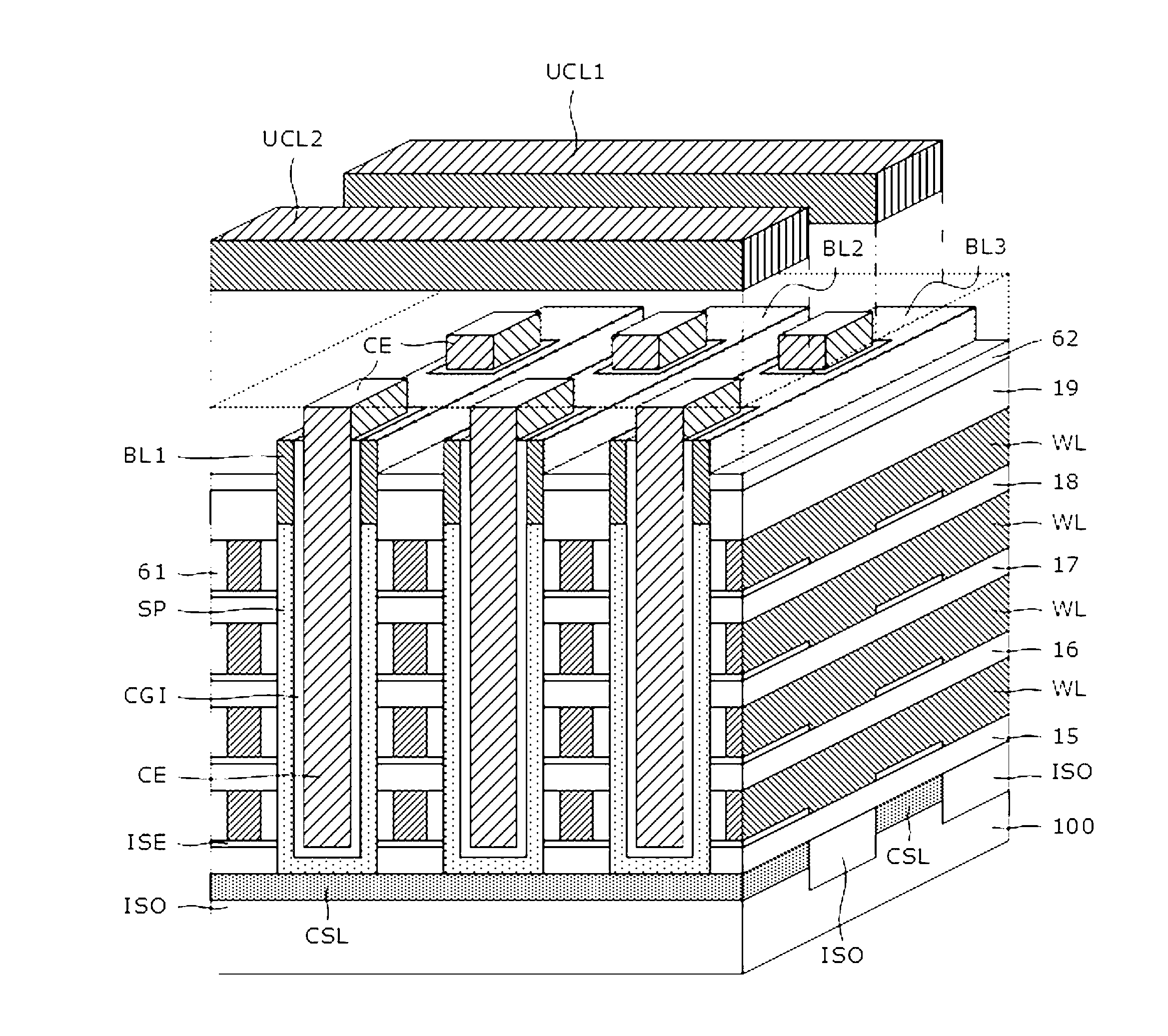
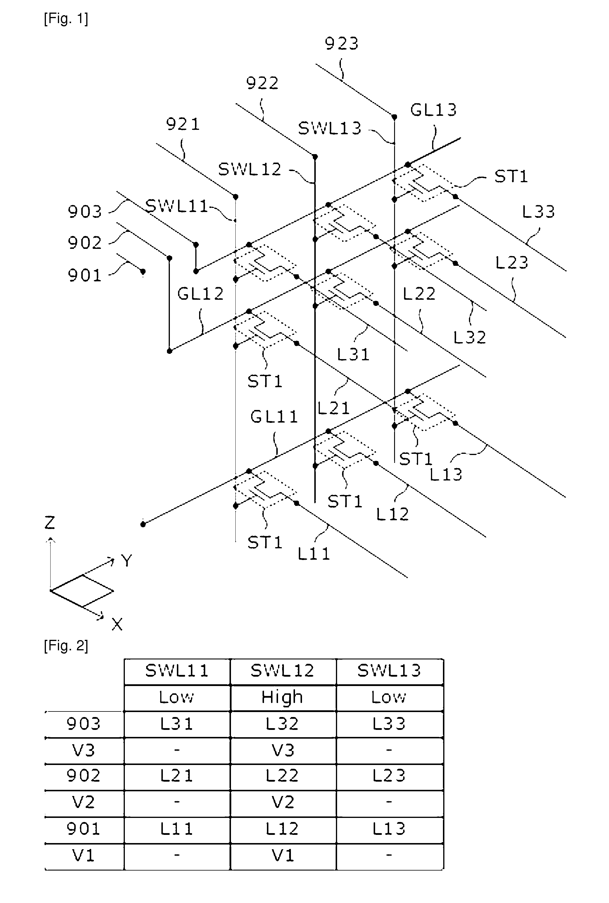
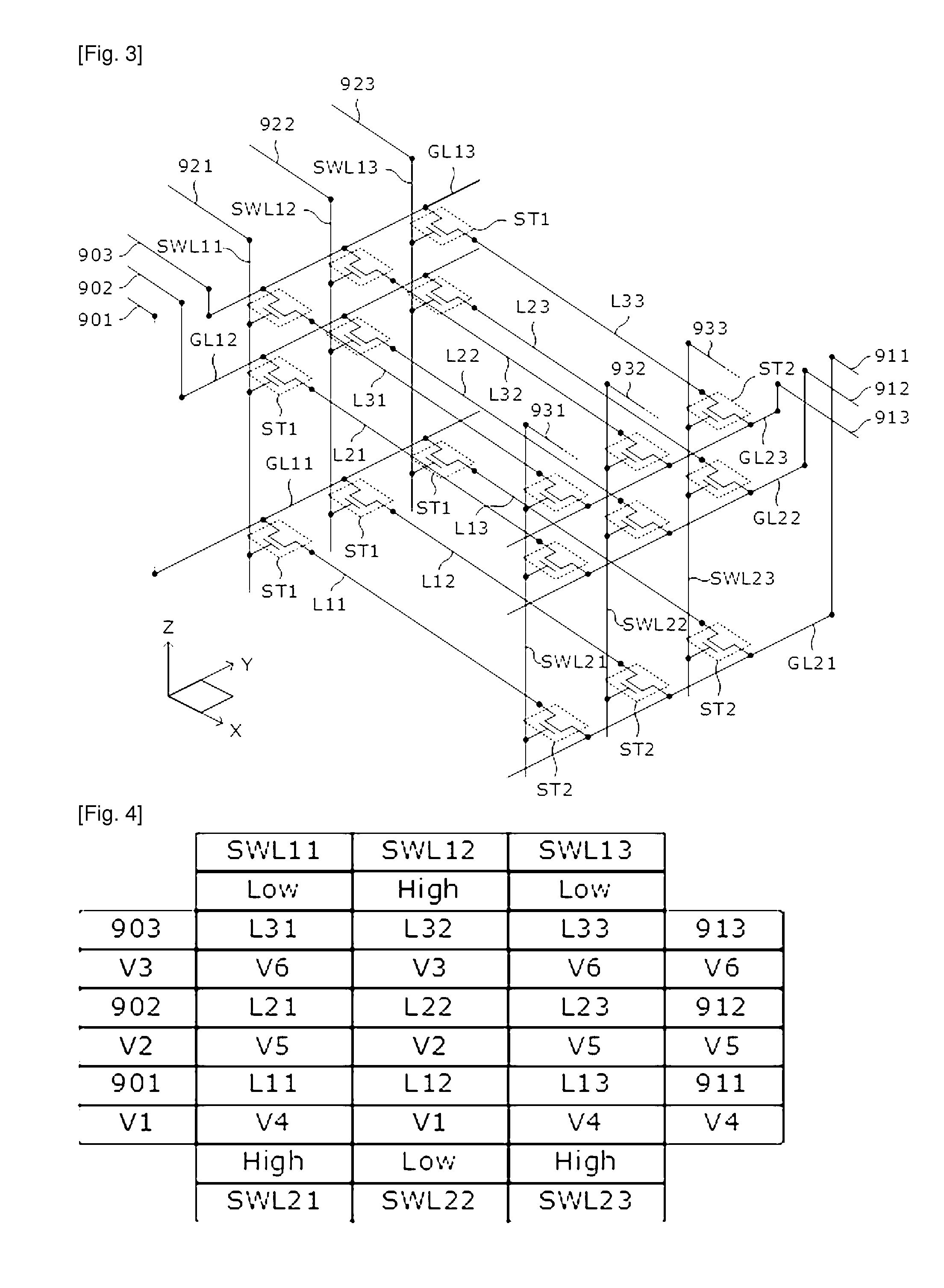
[0044]The objects, features, and advantages of the present invention will be apparent from the following detailed description of embodiments of the invention with references to the following drawings. However, the present invention is not limited to the exemplary embodiments disclosed below, but can be implemented in various types. Therefore, the present embodiments are provided for complete disclosure of the present invention and to fully inform the scope of the present invention to those ordinarily skilled in the art.

[0045]It will also be understood that when a layer is referred to as being “on” another layer or substrate, it can be directly on the other layer or substrate, or intervening layers may also be present. In the drawings, the thicknesses of layers and regions are exaggerated for clarity. It will be understood that, although the terms first, second, etc. may be used herein to describe various elements, components, regions, layers and / or sections, these elements, compon...


PUM


Abstract

Provided are three-dimensional semiconductor devices and methods of fabricating and operating the same. A device includes a connection node interposed between first and second nodes, a semiconductor pattern connected to the connection node, a plurality of memory elements connected to the semiconductor pattern, word lines connected to the memory elements, and a control electrode disposed opposite the semiconductor pattern. The control electrode selectively controls an electrical connection between the connection node and the memory element, thereby preventing an un-intended current path in a cross-point 3D memory device.

Description

TECHNICAL FIELD [0001]The present invention relates to a semiconductor device and methods of fabricating and operating the same.BACKGROUND ART [0002]In order to enable good performance and low price at consumers' request, it is necessary to increase the integration density of semiconductor devices. Above all, since the integration density of memory semiconductor devices significantly affects a product price, it is required to increase the integration density of the memory semiconductor devices. In the case of a typical two-dimensional or planar semiconductor memory device, since its degree of integration is largely determined by an area occupied by a unit memory cell, techniques used to form fine patterns have an effect on the integration degree and, therefore, the device cost. However, since expensive equipment is required for pattern miniaturization, even if the integration degree of a two-dimensional semiconductor memory device is increased, the semiconductor device is still unde...

Claims


Application Information

Patent Timeline
IPC IPC(8): H01L27/26
CPCG11C5/02H01L27/2481G11C11/5678G11C13/0004G11C13/0023G11C13/003G11C16/0408G11C16/0475G11C16/0483G11C2213/71G11C2213/75H01L27/11551H01L27/11556H01L27/11578H01L27/228H01L27/24G11C11/5671H10B61/22H10B63/34H10B63/84H10N70/823H10N70/8413H10N70/231H10B41/20H10B43/20H10B41/27H10B53/20H10B53/30H10B63/00
Inventor KIM, SUNG-DONG
Owner KIM SUNG DONG
Why Eureka
Try Eureka