
Automated Pin Multiplexing for Programmable Logic Device Implementation of Integrated Circuit Design

Active Publication Date: 2011-06-16
APPLE INC
View PDF34 Cites 17 Cited by
  • Summary
  • Abstract
  • Description
  • Claims
  • Application Information

AI Technical Summary

Benefits of technology

[0008]In some embodiments, the automation of pin multiplexing may reduce the errors that may occur when manual pin multiplexing is assigned by a user. Even one error in the assignment of signals to be multiplexed may result in a failure to generate a functional programmable logic device implementation. Automating the pin multiplexing assignment using clock domain tracing may frequently lead to functional programmable logic device implementations.

Problems solved by technology

Even one error in the assignment of signals to be multiplexed may result in a failure to generate a functional programmable logic device implementation.

Method used


Image

  • Automated Pin Multiplexing for Programmable Logic Device Implementation of Integrated Circuit Design
  • Automated Pin Multiplexing for Programmable Logic Device Implementation of Integrated Circuit Design
  • Automated Pin Multiplexing for Programmable Logic Device Implementation of Integrated Circuit Design

Examples


Embodiment Construction

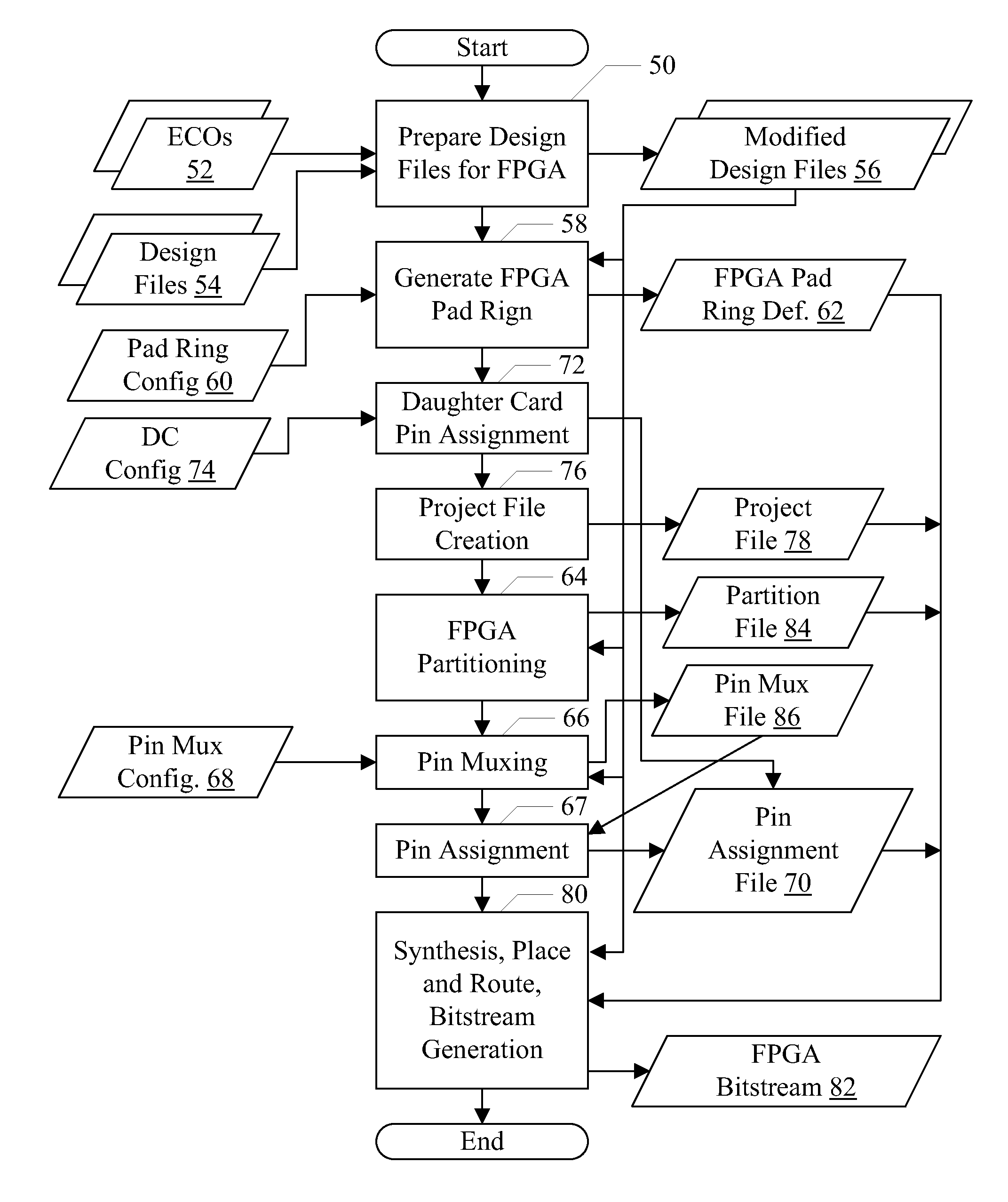
HDL Design File to Programmable Logic Device Methodology Overview

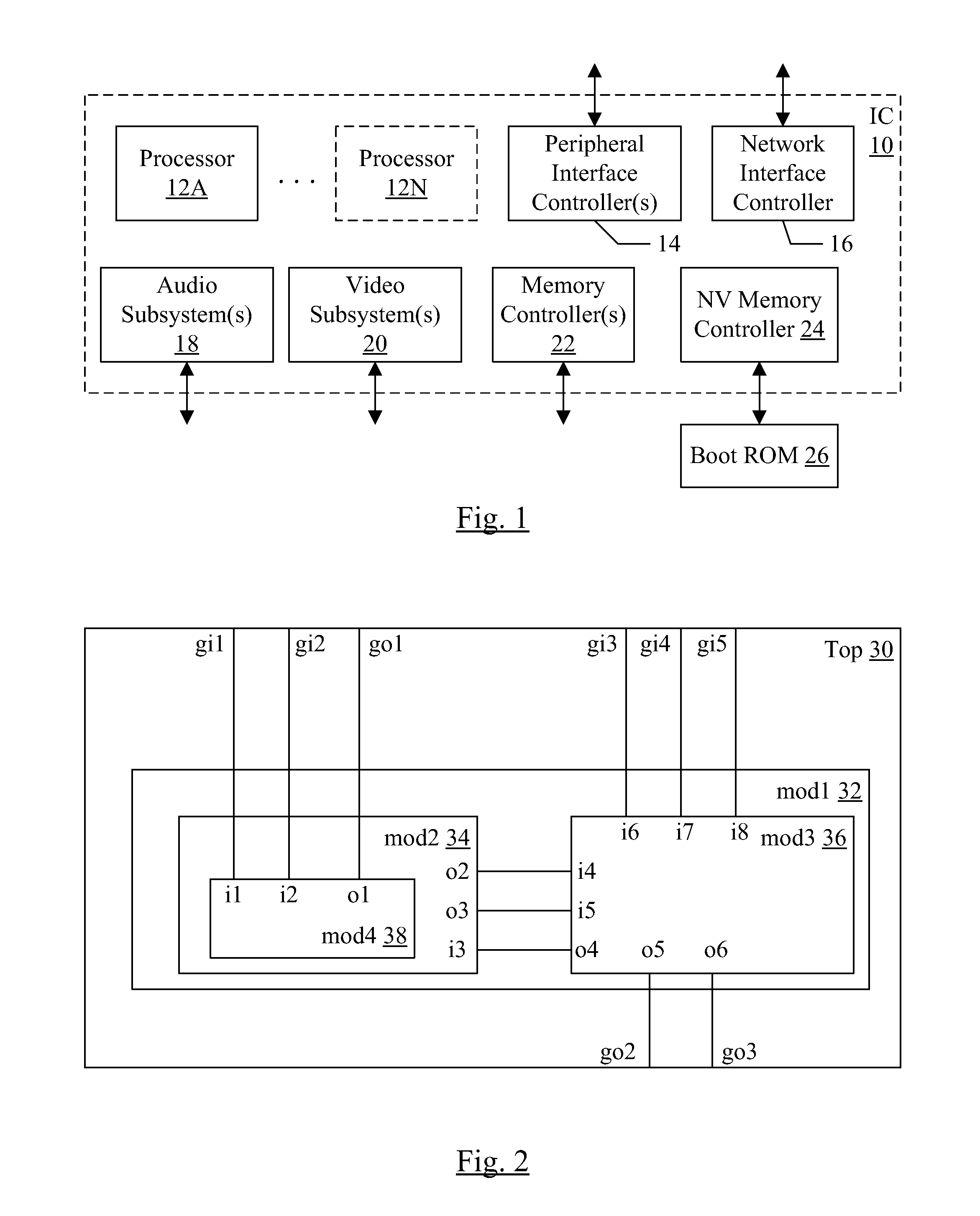
[0029]As mentioned above, the design of an integrated circuit may be described in one or more design files, using an HDL. Exemplary HDLs that may be used in various embodiments include Verilog, VHDL, etc. Generally, HDLs may support the description of the integrated circuit at a high level (e.g. as logic equations) that may be convenient for human generation and consumption. In one embodiment, the design descriptions may be register-transfer level (RTL) descriptions expressed in an HDL. The description in the design files, when taken as a whole, describe the integrated circuit. The division into multiple design files may provide for convenient editing and change tracking. For example, each component of the integrated circuit may be represented by one or more design files.

[0030]The design files may be processed in a variety of ways. For example, the design files may be compiled to a variety of target platforms for testi...


PUM


Abstract

In an embodiment, a method to automatically select groups of signals to be multiplexed on pins of a programmable logic device in a programmable logic device implementation of at least a portion of an integrated circuit is contemplated. The set of signals that may be candidates for multiplexing may be received (e.g., the set may be output by programmable logic device design tool). Clock domain tracing may be performed, and signals that have matching clock domains may be identified as candidates for multiplexing. Signals from matching clock domains may be grouped (up to a maximum number of signals that may be multiplexed on one pin) and assigned to pins of the programmable logic devices.

Description

BACKGROUND[0001]1. Field of the Invention[0002]This invention is related to the field of integrated circuit design and, more particularly, to implementing an integrated circuit design in one or more programmable logic devices.[0003]2. Description of the Related Art[0004]Integrated circuit design and testing continues to grow in complexity as the complexity of the integrated circuit itself increases. With every new generation of integrated circuit fabrication technology, the number of transistors that can be included on a given integrated circuit chip increases, which further contributes to the increased complexity.[0005]A programmable logic device implementation of all or portions of an integrated circuit design is one option that can be used during the development of an integrated circuit. Programmable logic device implementations typically operate at higher speeds than software simulations, permitting more extensive testing and / or more complex testing. For example, running the act...

Claims


Application Information

Patent Timeline
IPC IPC(8): G06F17/50
CPCG06F17/5054G06F30/34
Inventor CHEN, CHIH-ANG
Owner APPLE INC
Features
  • Generate Ideas
  • Intellectual Property
  • Life Sciences
  • Materials
  • Tech Scout
  • Unparalleled Data Quality
  • Higher Quality Content
  • 60% Fewer Hallucinations
Learn More