

Directional coupler
- Summary
- Abstract
- Description
- Claims
- Application Information
AI Technical Summary
Benefits of technology
Problems solved by technology
Method used
Image

Examples
example 1
2. Inventive Example 1
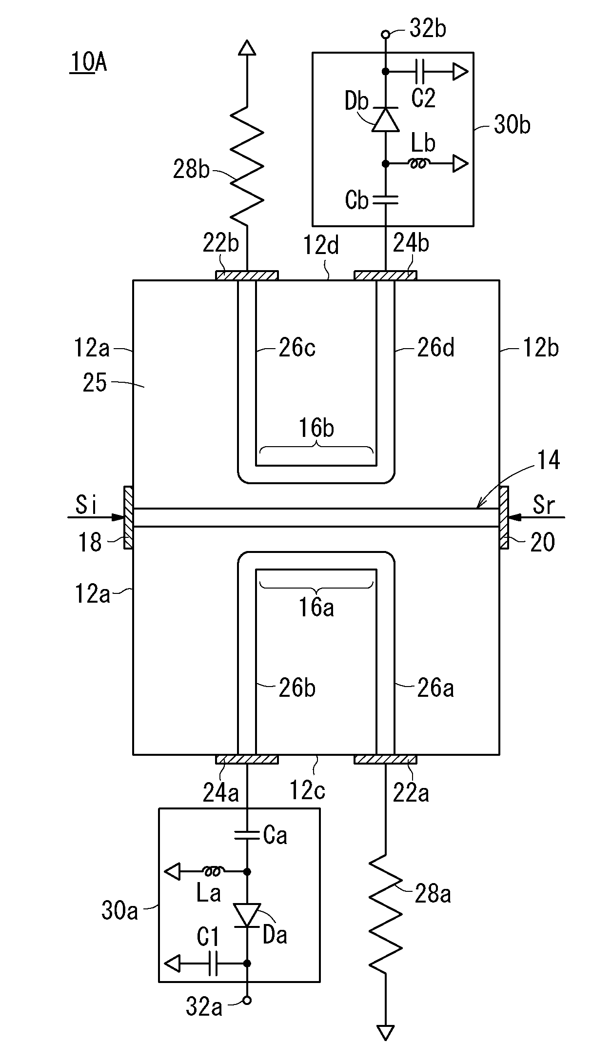
[0146]An inner layer conductive pattern as shown in FIG. 4 was printed using a silver paste on a ceramics green sheet of ceramics having a dielectric constant of 7. A prescribed number of such ceramics green sheets were compressed and stacked together, and then fired at about 950° C. Then, terminal electrodes were printed on the four side faces, thus fabricating an integral first directional coupler 10A as shown in FIG. 3.
[0147]The fabricated first directional coupler 10A had a vertical dimension of 7.0 mm, a horizontal dimension of 14.0 mm, and a thickness of 2.5 mm. The first directional coupler disposed in one dielectric substrate 12 had a first coupling and a second coupling each of 30 dB, a first isolation and a second isolation each of 60 dB, and had an insertion loss of 0.09 dB because of its main line 14.
[0148]The first directional coupler 10A was mounted on a wiring board as shown in FIG. 5.
[0149]A signal of −30 dB (input monitor signal Sia) output fro...
PUM
 Abstract
Description
Claims
Application Information