
Imaging device and method for sharing memory among chips

Inactive Publication Date: 2011-06-23
MTEKVISION CO LTD
View PDF4 Cites 36 Cited by
  • Summary
  • Abstract
  • Description
  • Claims
  • Application Information

AI Technical Summary

Benefits of technology

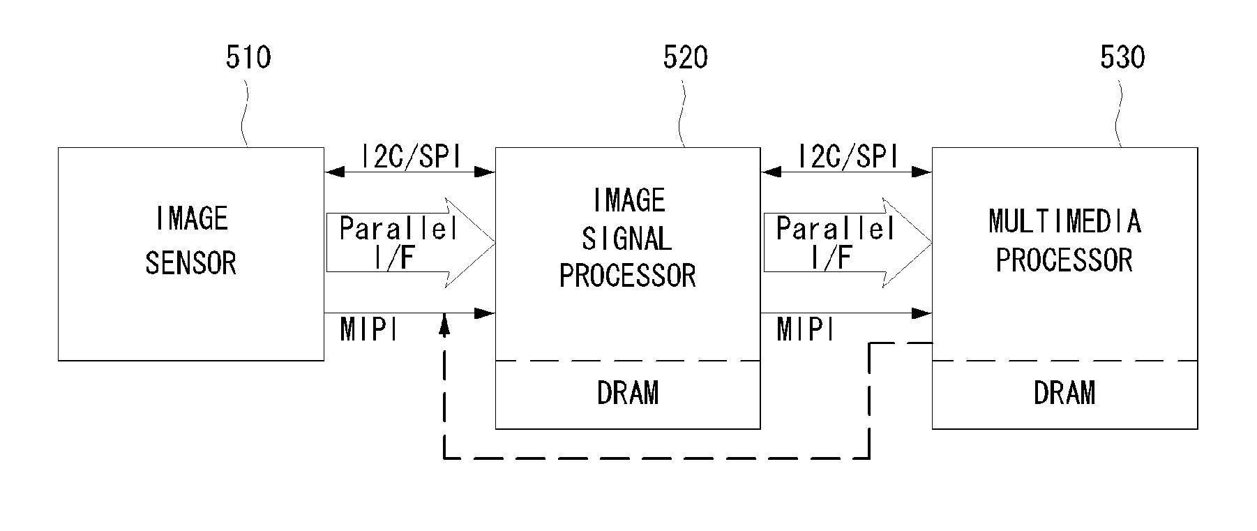
[0017]An advantage of some aspects of the invention is that it provides an imaging device and a memory sharing method, which can efficiently utilize resources in a mobile communication terminal having a camera function.
[0018]Another advantage of some aspects of the invention is that it provides an imaging device and a memory sharing method, which can allow another chip (for example, one or more of a baseband chip and a multimedia processor chip) to utilize a memory shared to perform additional functions, by allowing another chip to efficiently share a memory (for example, DRAM) in an image signal processor chip of a mobile communication terminal having a camera function when the image signal processor chip is not used.
[0037]According to the above-mentioned configurations, it is possible to efficiently utilize resources in a mobile communication terminal having a camera function.
[0038]It is also possible to allow another chip (for example, one or more of a baseband chip and a multimedia processor chip) to utilize a memory shared to perform additional functions, by allowing another chip to efficiently share a memory (for example, DRAM) in an image signal processor chip of a mobile communication terminal having a camera function when the image signal processor chip is not used.

Problems solved by technology

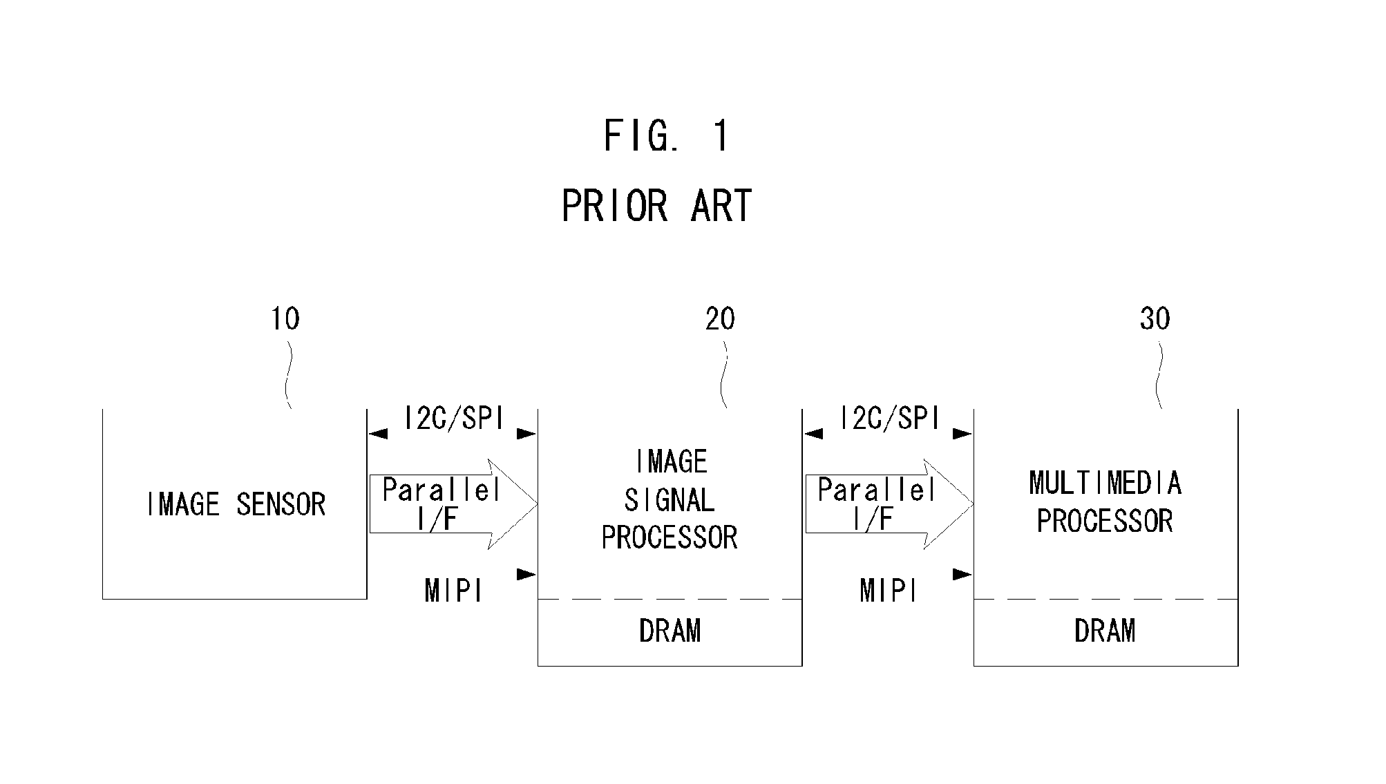
However, in the mobile communication terminal having a camera function according to the related art, when the image signal processor chip is not activated, there is not suggested an effective method of allowing another chip to utilize the memory in the image signal processor chip.

Method used


Image

  • Imaging device and method for sharing memory among chips
  • Imaging device and method for sharing memory among chips
  • Imaging device and method for sharing memory among chips

Examples


Embodiment Construction

[0045]The invention can be variously modified in various forms and specific embodiments will be described and shown in the drawings. However, the embodiments are not intended to limit the invention, but it should be understood that the invention includes all the modifications, equivalents, and replacements belonging to the spirit and the technical scope of the invention. When it is determined that detailed description of known techniques associated with the invention makes the gist of the invention obscure, the detailed description will be omitted.

[0046]Terms such as “first” and “second” can be used to describe various elements, but the elements are not limited to the terms. The terms are used only to distinguish one element from another element.

[0047]The terms used in the following description are used to merely describe specific embodiments, but are not intended to limit the invention. An expression of the singular number includes an expression of the plural number, so long as it ...


PUM


Abstract

An imaging device and a memory sharing method are provided. The imaging device includes: an image sensor; an image signal processor chip that includes a frame memory and that receives and processes a video signal from the image sensor; and a control processor chip that receives video information from the image signal processor chip via a first serial interface and that accesses the frame memory via a second serial interface used for the image signal processor chip to receive the video image signal from the image sensor. Accordingly, it is possible to efficiently utilize resources in a movable communication terminal having a camera function.

Description

CROSS REFERENCE[0001]This application is based on and claims priority under 35USC 119 from Korean Patent Application No. 10-2009-0125937, filed on Dec. 17, 2009.BACKGROUND[0002]1. Field of the Invention[0003]The present invention relates to an imaging device, and more particularly, to an imaging device and a memory sharing method between chips.[0004]2. Description of the Related Art[0005]Recently, various imaging devices such as a mobile communication terminal having a camera function and a digital camera have been developed. In the mobile communication terminal having a camera function, various chips provided to carry out the camera function are not always activated but the activations thereof are determined depending on their functions.[0006]FIG. 1 is a sectional view of a mobile communication terminal having a camera function according to the related art.[0007]Referring to FIG. 1, the mobile communication terminal having a camera function includes an image sensor 10, an image sig...

Claims


Application Information

Patent Timeline
IPC IPC(8): H04N5/907
CPCH04N5/335H04N25/00G06T1/00H04N23/00
Inventor KIM, WANG-HYUN
Owner MTEKVISION CO LTD
Learn More