Device, system, and method for reducing program/read disturb in flash arrays

a technology of flash arrays and devices, applied in the field of devices, systems and methods for reducing program/read disturb in flash arrays, can solve problems such as random distortion of measured levels

Active Publication Date: 2011-06-23
AVAGO TECH INT SALES PTE LTD
View PDF102 Cites 123 Cited by
  • Summary
  • Abstract
  • Description
  • Claims
  • Application Information

AI Technical Summary

Problems solved by technology

Due to inaccuracies during the programming procedure and charge loss due to time and temperature (also known as retention), the measured levels may suffer from a random distortion.

Method used


Image

  • Device, system, and method for reducing program/read disturb in flash arrays
  • Device, system, and method for reducing program/read disturb in flash arrays
  • Device, system, and method for reducing program/read disturb in flash arrays

Examples


Embodiment Construction

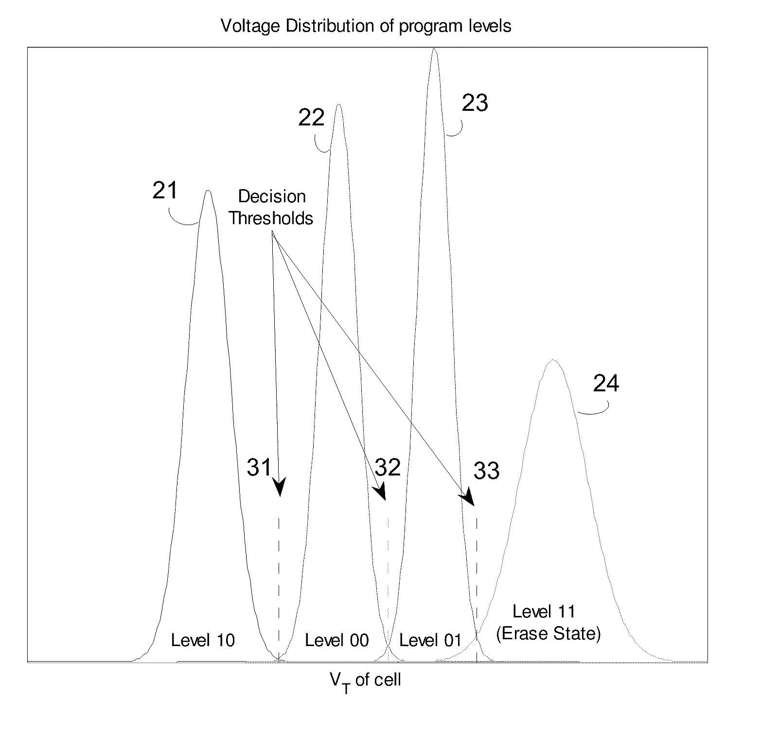
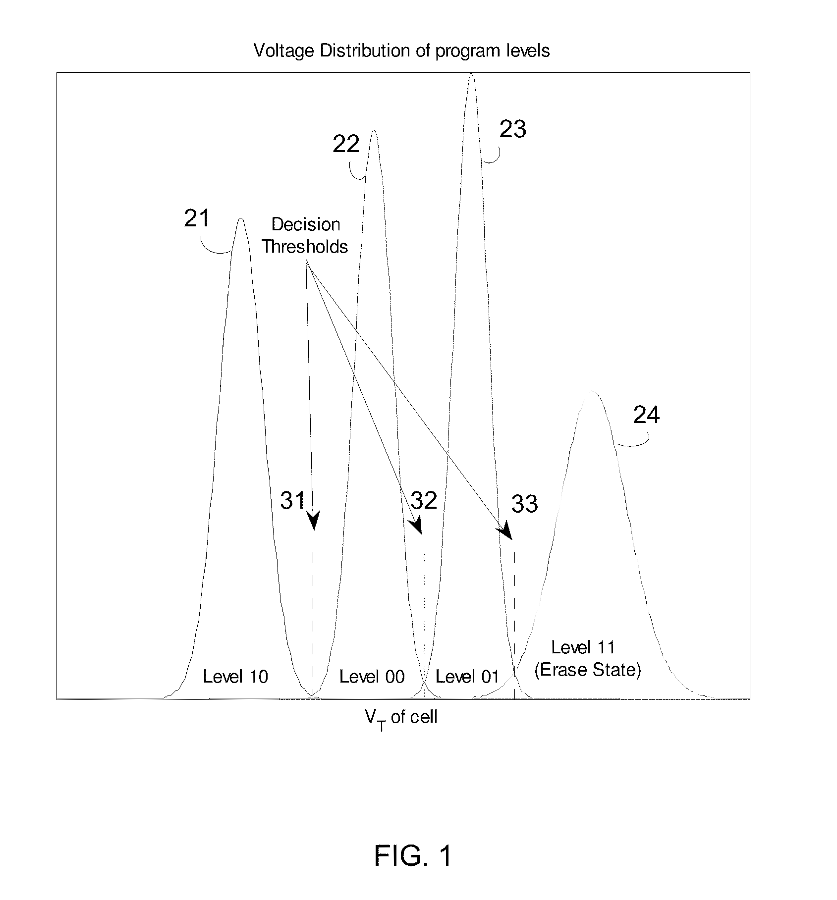
The subject matter regarded as the invention is particularly pointed out and distinctly claimed in the concluding portion of the specification. The invention, however, both as to organization and method of operation, together with objects, features, and advantages thereof, may best be understood by reference to the following detailed description when read with the accompanying drawings.

It will be appreciated that for simplicity and clarity of illustration, elements shown in the figures have not necessarily been drawn to scale. For example, the dimensions of some of the elements may be exaggerated relative to other elements for clarity. Further, where considered appropriate, reference numerals may be repeated among the figures to indicate corresponding or analogous elements.

In the following detailed description, numerous specific details are set forth in order to provide a thorough understanding of the invention. However, it will be understood by those skilled in the art that the pre...


PUM


Abstract

A method, device and computer readable medium for programming a nonvolatile memory block. The method may include programming information, by a memory controller, to the nonvolatile memory block by performing a sequence of programming phases of descending bit significances. The device may include a nonvolatile memory block; and a memory controller that may be configured to determine a bit significance level of the nonvolatile memory block; program the nonvolatile memory block by performing at least one programming phase; and program the nonvolatile memory block to an erase value that may be higher than the pre-erase value; wherein the erase value and the pre-erase value may be selected based on the bit significance level of the nonvolatile memory block. The method may include packing three single level cell (SLC) nonvolatile memory blocks to one three-bit per cell nonvolatile memory block in order of the three SLC bit significances.

Description

BACKGROUNDModern flash memory devices may store information as charge in cells, where each cell may be made of a floating gate transistor or an NROM transistor. In single-level cell (SLC) flash memory devices, each cell may store only one bit of information. Multi-level cell (MLC) flash memory devices can store more than one bit per cell by choosing between more than one pair of levels of electrical charge to apply to the floating gates of their cells. The applied charge (also known as charge level) may be measured by a detector. The detector may compare the voltage of the transistor gate (also known as charge level and denoted VT) to a decision threshold voltage (also known as charge level boundary point and denoted VD). The amount of charge may be used to determine the programmed level (logical value) of the cell. Due to inaccuracies during the programming procedure and charge loss due to time and temperature (also known as retention), the measured levels may suffer from a random ...

Claims


Application Information

Patent Timeline
Patent Type & Authority Applications(United States)
IPC IPC(8): G06F13/28
CPCG11C11/5628G11C2211/5648G11C16/3495
Inventor SABBAG, EREZ
Owner AVAGO TECH INT SALES PTE LTD
Why Eureka
Try Eureka