Manufacturing method for light emitting device

a manufacturing method and light-emitting technology, applied in the field of manufacturing methods for light-emitting devices, can solve problems such as the reduction of luminance performance, and achieve the effect of increasing the quantity of light emerging from the sapphire layer

Active Publication Date: 2011-06-30
DISCO CORP
View PDF2 Cites 11 Cited by
  • Summary
  • Abstract
  • Description
  • Claims
  • Application Information

AI Technical Summary

Benefits of technology

[0008]It is therefore an object of the present invention to provide a manufacturing method for a light emitting device which can efficiently emerge the light from the sapphire layer to exhibit a high luminance performance.
[0010]According to the present invention, a plurality of light emitting devices are manufactured so that each light emitting device has a structure that a light emitting layer is formed on the front side of a sapphire layer divided from the sapphire substrate layer of the light emitting device wafer. The sapphire layer of each light emitting device manufactured by the present invention is surrounded by a plurality of side surfaces formed by cutting the sapphire substrate layer of the wafer along the processed locus formed by the laser processing, and the sectional shape of each side surface of the sapphire layer is a corrugated or zigzag shape corresponding to the processed locus. Accordingly, although the incident angle of light incident on one side surface in the sapphire layer is greater than a critical angle to cause the total reflection on this side surface, the incident angle of the totally reflected light next incident on another side surface in the sapphire layer or further next incident on another side surface in the sapphire layer tends to become less than the critical angle and accordingly pass through this side surface. As a result, the quantity of light emerging from the sapphire layer can be increased.

Problems solved by technology

Thus, the light emitted from the light emitting layer cannot be efficiently emerged from the sapphire layer, causing a reduction in luminance performance.

Method used


Image

  • Manufacturing method for light emitting device
  • Manufacturing method for light emitting device
  • Manufacturing method for light emitting device

Examples


Embodiment Construction

[0029]A preferred embodiment of the present invention for dividing a light emitting device wafer to obtain a plurality of light emitting devices will now be described with reference to the drawings.

(1) Light Emitting Device Wafer

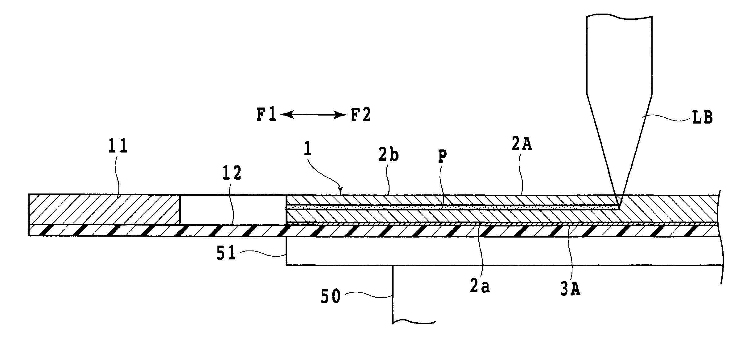
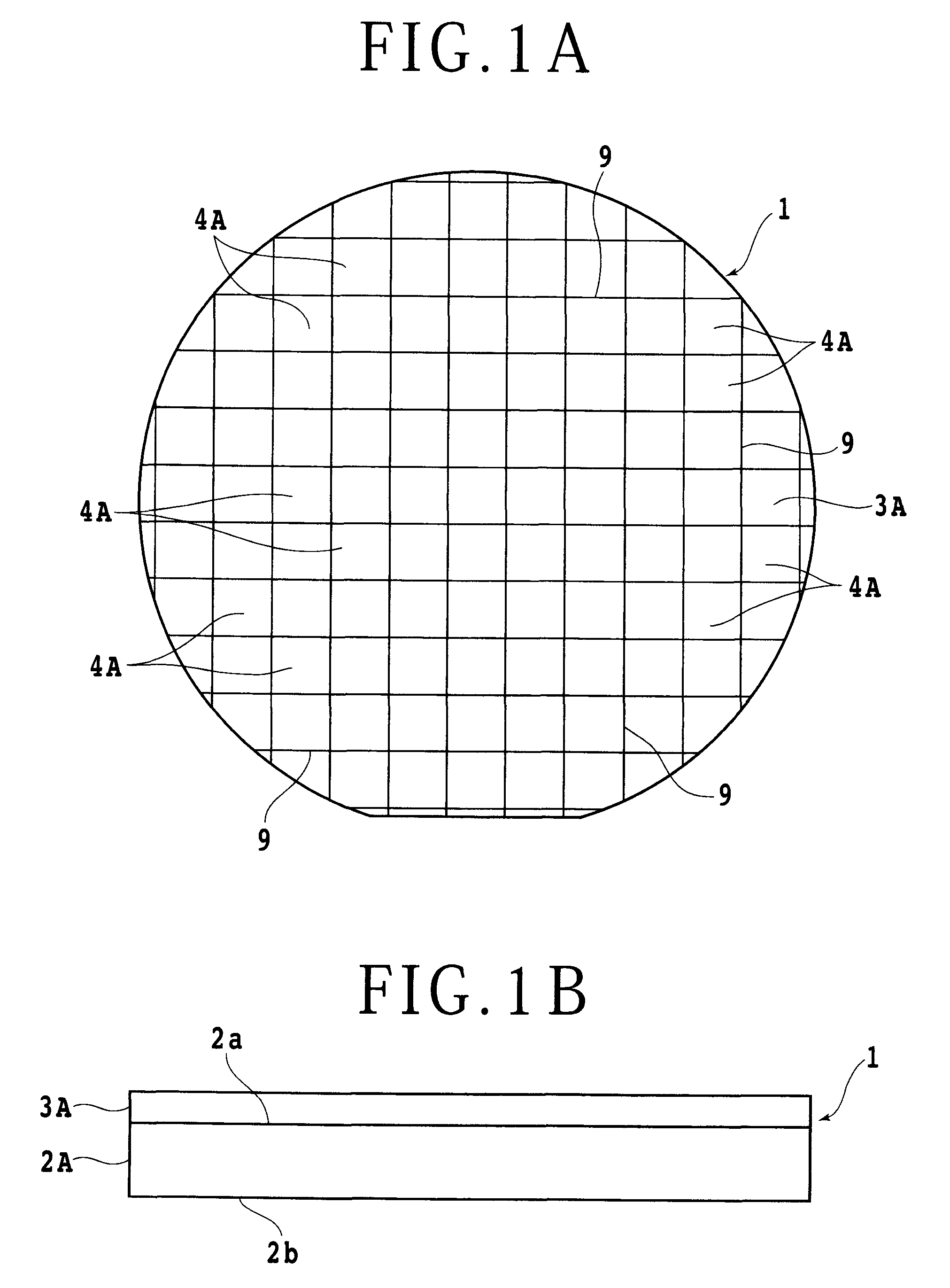
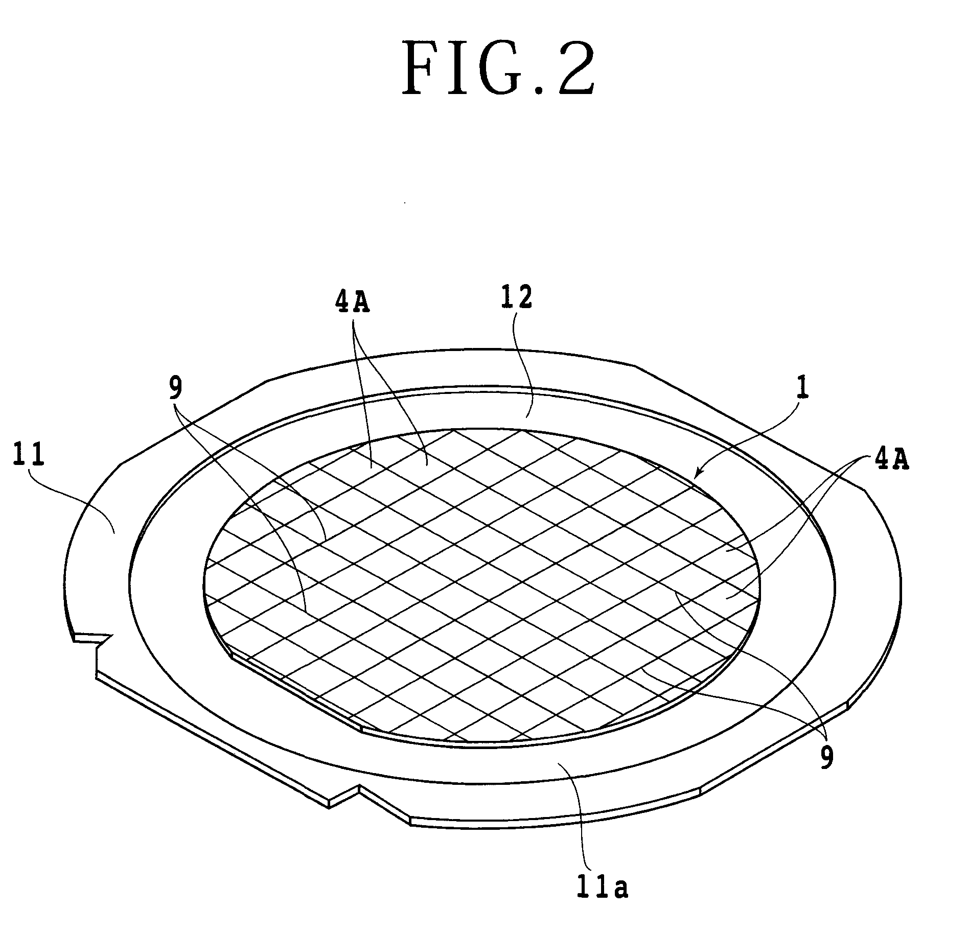
[0030]FIG. 1A is a plan view of a light emitting device wafer 1 according to an embodiment of the present invention and FIG. 1B is a side view of the light emitting device wafer 1 shown in FIG. 1A. As shown in FIG. 1B, the light emitting device wafer 1 is composed of a disk-shaped sapphire substrate layer 2A having a front surface (upper surface as viewed in FIG. 1B) 2a and a back surface 2b and a light emitting layer 3A formed on the whole front surface 2a of the sapphire substrate layer 2A. As shown in FIG. 1A, a plurality of crossing straight division lines 9 are formed on the light emitting layer 3A to thereby partition a plurality of rectangular light emitting device areas 4A.

[0031]The light emitting layer 3A is of such a kind as well known in the art, ...


PUM

PropertyMeasurementUnit
incident angleaaaaaaaaaa
lengthaaaaaaaaaa
external forceaaaaaaaaaa

Abstract

A light emitting device manufacturing method including the steps of corrugatedly scanning a laser beam along a plurality of division lines formed on a light emitting device wafer having a sapphire substrate layer and a light emitting layer to apply the laser beam to the sapphire substrate layer, thereby performing laser processing for the sapphire substrate layer and next applying an external force to a processed locus formed along each division line by the above laser processing to thereby divide the light emitting device wafer into a plurality of light emitting devices. The sapphire layer of each light emitting device has side surfaces whose horizontal sectional shape is a corrugated shape. Accordingly, the number of total reflections on the side surfaces of the sapphire layer can be reduced to thereby achieve efficient emergence of light from the sapphire layer.

Description

BACKGROUND OF THE INVENTION[0001]1. Field of the Invention[0002]The present invention relates to a method of manufacturing a plurality of light emitting devices by dividing a light emitting device wafer having a sapphire substrate layer and a light emitting layer.[0003]2. Description of the Related Art[0004]In a semiconductor device fabrication process, a plurality of crossing division lines are formed on the front side of a substantially disk-shaped semiconductor wafer to thereby partition a plurality of regions where devices having electronic circuits such as ICs and LSIs are respectively formed. The semiconductor wafer is cut along the division lines to thereby divide the regions where the devices are formed from each other, thus obtaining the individual devices as a plurality of semiconductor chips. Further, a light emitting device wafer is provided by forming a plurality of light emitting devices such as light emitting diodes (LEDs) on the front side of a sapphire substrate. Th...

Claims


Application Information

Patent Timeline
Patent Type & Authority Applications(United States)
IPC IPC(8): H01L33/08B23K26/00B28D5/00
CPCB23K26/0057B23K26/367B23K26/4075B23K26/409H01L33/22B28D5/0011H01L21/67092H01L33/0095H01L33/20B23K2201/40B23K26/364B23K26/40B23K26/53B23K2101/40B23K2103/172B23K2103/50
Inventor ENDO, TOMOHIRO
Owner DISCO CORP
Why Eureka
Try Eureka