

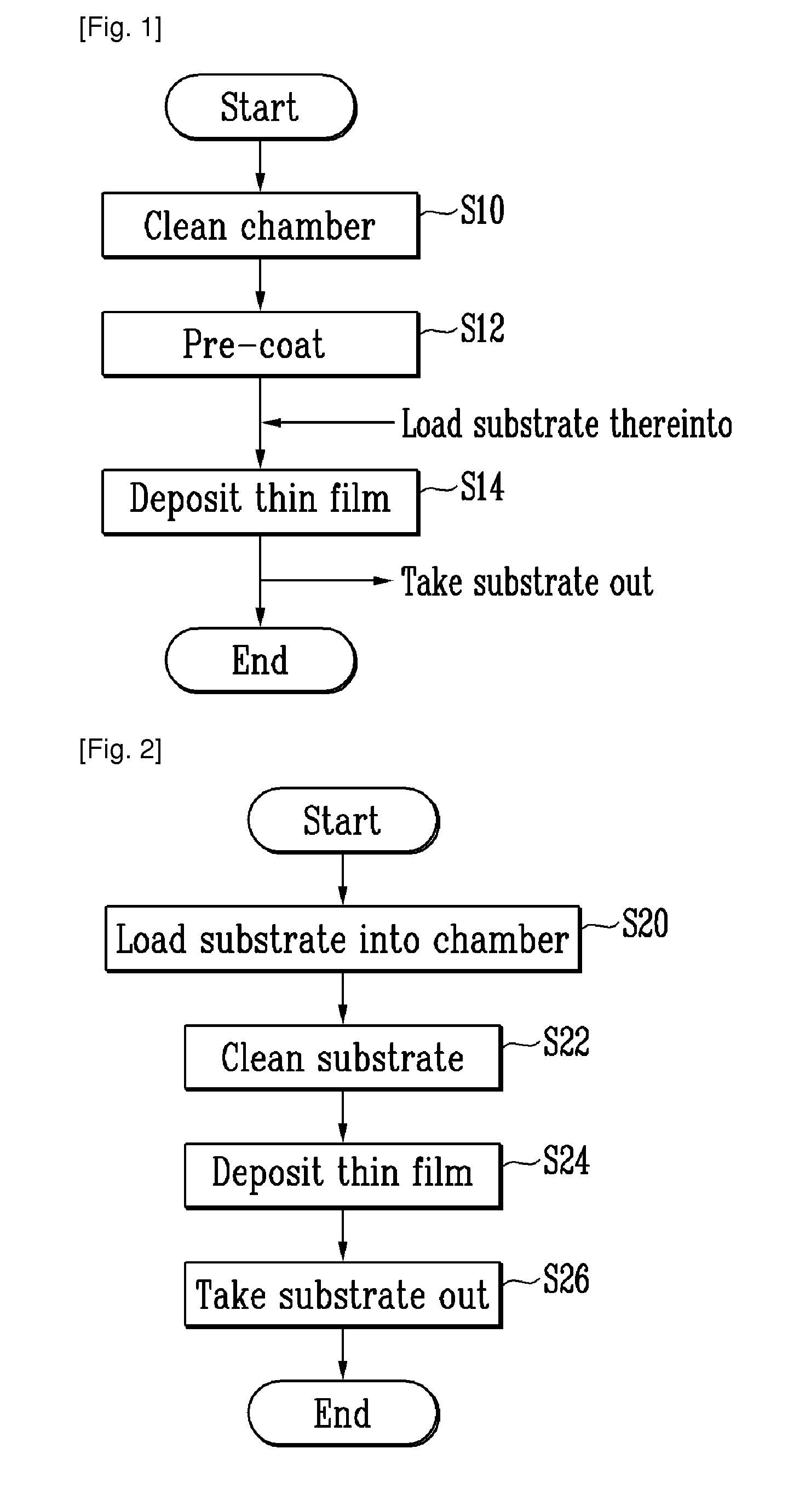
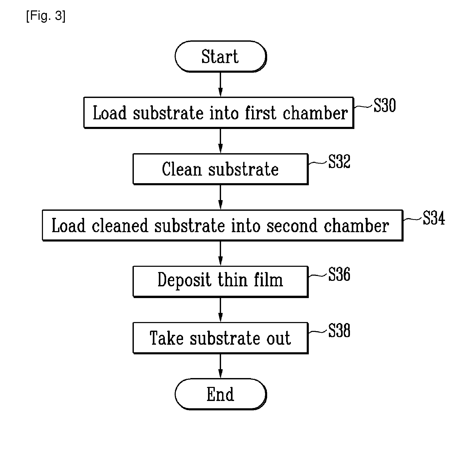
Method for depositing amorphous silicon thin film by chemical vapor deposition
a technology amorphous silicon, which is applied in chemical vapor deposition coating, coating, metallic material coating process, etc., can solve the problems that the conventional method of chemical vapor deposition cannot prevent the formation of silicon nitride or silicon oxide substrates, and the formation of bubble defects when amorphous silicon thin film is deposited on contaminated silicon, so as to increase the yield of various electronic devices manufactured using amorphous silicon
- Summary
- Abstract
- Description
- Claims
- Application Information
AI Technical Summary
Benefits of technology
Problems solved by technology
Method used
Image

Examples
example 1
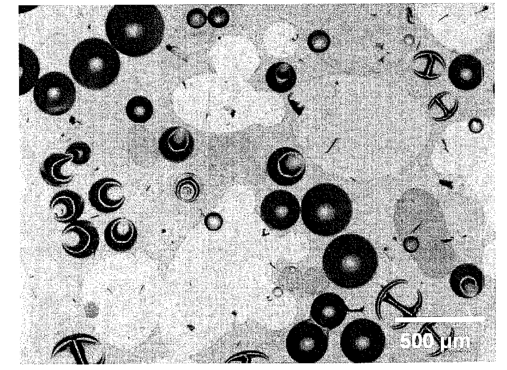
[0045]A silicon nitride (Si3N4) thin film was deposited on a silicon wafer to a thickness of 100 nm and exposed to air for 5 minutes. Then, the silicon wafer was introduced into a chamber cleaned with a fluorine-containing gas and coated with amorphous silicon deposited to a thickness of 150 nm using SiH4, and cleaned with ammonia (NH3) gas activated by plasma due to supply of RF power. Here, the cleaning was performed at a substrate temperature of 400° C., a gas flow of 100 sccm, a chamber pressure of 0.8 Torr, and an RF power of 0.3 W / cm2, for 5 minutes. Subsequently, an amorphous silicon thin film was subsequently deposited to a thickness of 150 nm using SiH4 gas without a vacuum break. Here, the deposition of the amorphous silicon thin film was performed at a substrate temperature of 400° C., a gas flow of 30 sccm, a chamber pressure of 1.2 Torr, and an RF power of 0.1 W / cm2, for 4 minutes.
[0046]Finally, the deposited surface of the substrate was imaged by using optical microsco...
example 2
[0047]A silicon nitride (Si3N4) thin film was deposited on a silicon wafer to a thickness of 100 nm and exposed to air for 5 minutes. Then, the silicon wafer was introduced into a chamber cleaned with a fluorine-containing gas and coated with amorphous silicon deposited to a thickness of 150 nm using SiH4, and cleaned with ammonia (NH3) gas activated by plasma due to supply of RF power. Here, the cleaning was performed at a substrate temperature of 400° C., a gas flow of 100 sccm, a chamber pressure of 0.8 Torr, and an RF power of 0.3 W / cm2, for 5 minutes. Subsequently, an amorphous silicon thin film was deposited to a thickness of 150 nm using SiH4 gas including PH3 without a vacuum break. Here, the deposition of the amorphous silicon thin film was performed at a substrate temperature of 400° C., a SiH4 gas flow of 30 sccm, a flow of 1.5% PH3 gas diluted in H2 of 60 sccm, a chamber pressure of 1.2 Torr, and an RF power of 0.1 W / cm2, for 4 minutes.
[0048]Finally, the deposited surfac...
PUM
| Property | Measurement | Unit |
|---|---|---|
| pressure | aaaaa | aaaaa |
| temperature | aaaaa | aaaaa |
| pressure | aaaaa | aaaaa |
Abstract
Description
Claims
Application Information