

Lead, wiring member, package component, metal component with resin, resin-encapsulated semiconductor device, and methods for producing the same
a technology of resin-encapsulated semiconductor devices and wiring components, which is applied in the direction of plastic/resin/waxes insulators, solid-state devices, basic electric elements, etc., can solve the problems of negative influence on the solderability and appearance of wiring, and achieve the effects of preventing the discoloration of ag coatings, improving heat-resistant coefficients of organic coatings, and high stability
- Summary
- Abstract
- Description
- Claims
- Application Information
AI Technical Summary
Benefits of technology
Problems solved by technology
Method used
Image

Examples
embodiment 1
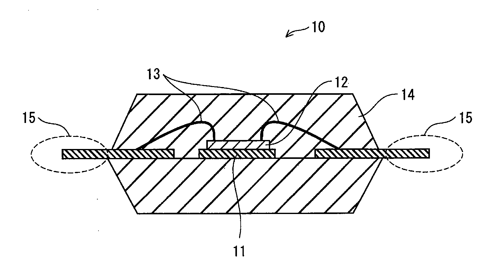
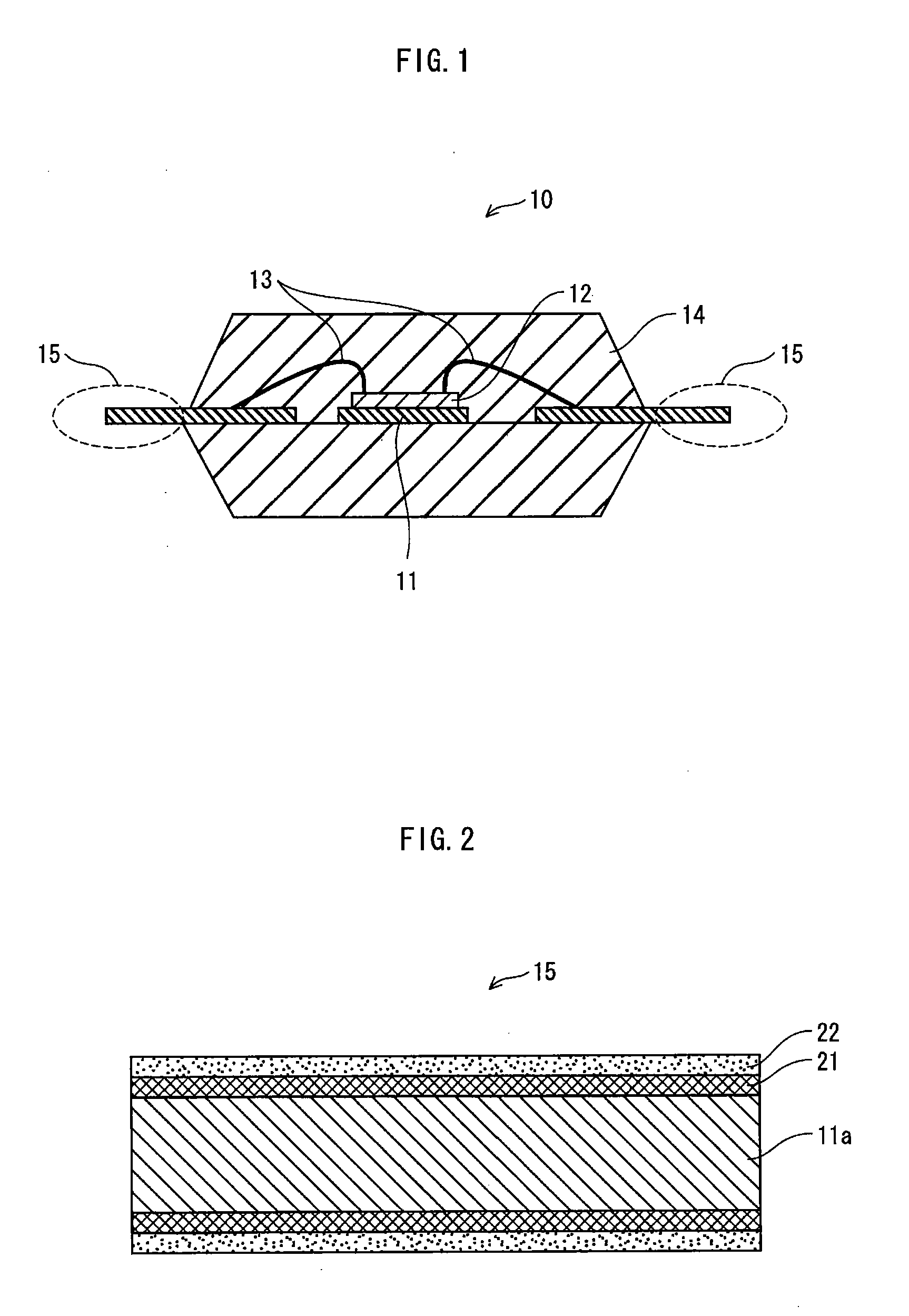
[0136]FIG. 1 is a sectional view of the structure of a semiconductor device 10 pertaining to the present embodiment. The semiconductor device 10 is a surface-mounted semiconductor device used in an IC, LSI etc., and is composed of a wiring lead 11, a semiconductor element 12, a wire 13 for electrical connection, and a resin body 14 as shown in FIG. 1.
(Wiring Lead 11)
[0137]The wiring lead 11 has a structure in which a surface of a metal plate 11a, composed of such metals as copper, copper alloy, steel and steel alloy, is coated with a metal coating 21 (refer to FIG. 2).
[0138]The metal coating 21 is composed of at least one layer of such metals as nickel, palladium, tin, copper, silver and gold, and is formed on the surface of the wiring lead by wet or dry plating.
[0139]It is exemplary that an outermost layer of the metal coating 21 is either one of silver, gold, and copper.
(Semiconductor Element 12)
[0140]The semiconductor element 12 is mounted on the wiring lead 11 by die bonding, an...
embodiment 2
1. Structure of the Semiconductor Device
[0201]FIG. 8A is an external perspective view showing a structure of a semiconductor device 10 pertaining to embodiment 2. FIG. 8B is a y-z cross-sectional view of the semiconductor device 10. FIG. 8C is an enlarged view of portion S1 in FIG. 8B.
[0202]The semiconductor device 10 is similar to the semiconductor device of embodiment 1, and is a surface-mounted semiconductor device QFP (Quad Flat Package) used in an IC, LSI etc., and is composed of a semiconductor chip 4, a wiring lead 3, wire 5, a resin body 121 molded to have a square form, and etc.
[0203]The wiring lead 3 is punched out of a metal plate constituted from a metal that has superior electrical conductivity (e.g., copper alloy), and includes die-pads 3a and 3b. Further, outer leads 301a which are a part of the die-pads 3a extend out from a circumference of the resin body 121.
[0204]As shown in FIG. 8B, the resin body 121 has an internal structure in which the semiconductor chip 4 has...
embodiment 3
[0256]In the present embodiment, description will be made on an LED device that includes a light emitting diode (LED) element.
[0257]FIG. 12 is a schematic cross-sectional view showing a structure of a wiring lead 35 and a reflector 122 of an LED device unit 36x of embodiment 3.
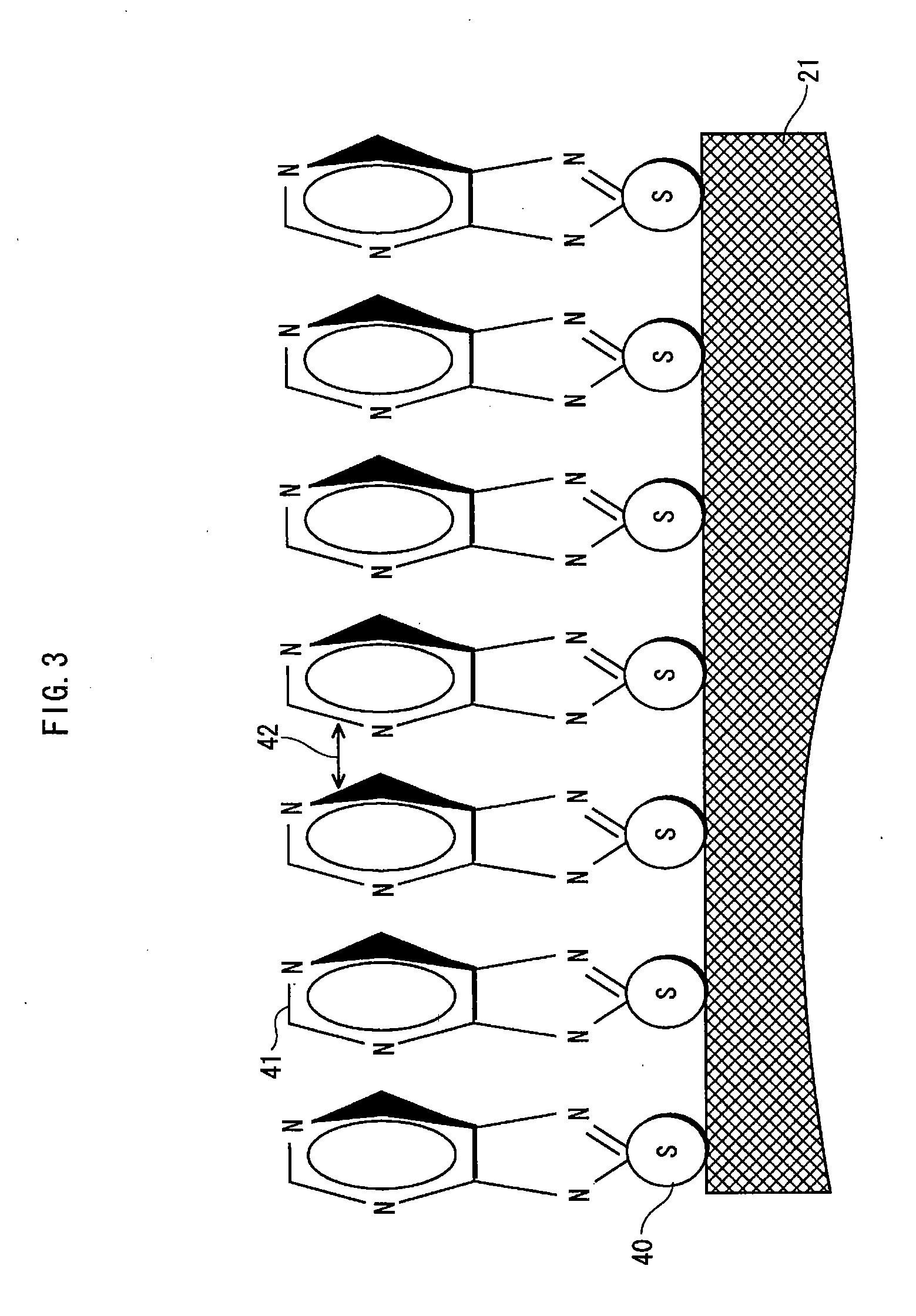
[0258]The LED device unit 36x has a structure where a wiring lead 35 has been provided on a bottom portion of a mortar-shaped reflector 122. The reflector 122 is formed by resin-molding a thermosetting resin material (e.g., epoxy resin). Similarly, the reflector 122 may also be formed by using ceramics material.
[0259]Similar to embodiment 1, there is a possibility of resin burrs forming in the LED device unit 36x as well. Specifically, areas 301 and 302 of the wiring lead 35 that are exposed at the bottom of the reflector 122 must retain electrical conductivity since an LED chip 42 is to be mounted thereupon later (refer to FIG. 13B). However, resin burrs can form on the exposed areas 301 and 302, by resin mat...
PUM
| Property | Measurement | Unit |
|---|---|---|
| temperature | aaaaa | aaaaa |
| chemical structure | aaaaa | aaaaa |
| polar | aaaaa | aaaaa |
Abstract
Description
Claims
Application Information