

Pellicle frame and pellicle containing same
a technology of pellicle and frame, which is applied in the direction of originals for photomechanical treatment, synthetic resin layered products, instruments, etc., can solve the problems of poor dimensional accuracy, poor quality and appearance, and anodized layer formed on the aluminum alloy surface, etc., to achieve moderate film strength, less sulfuric acid, and less haze
- Summary
- Abstract
- Description
- Claims
- Application Information
AI Technical Summary
Benefits of technology
Problems solved by technology
Method used
Image

Examples
example 1
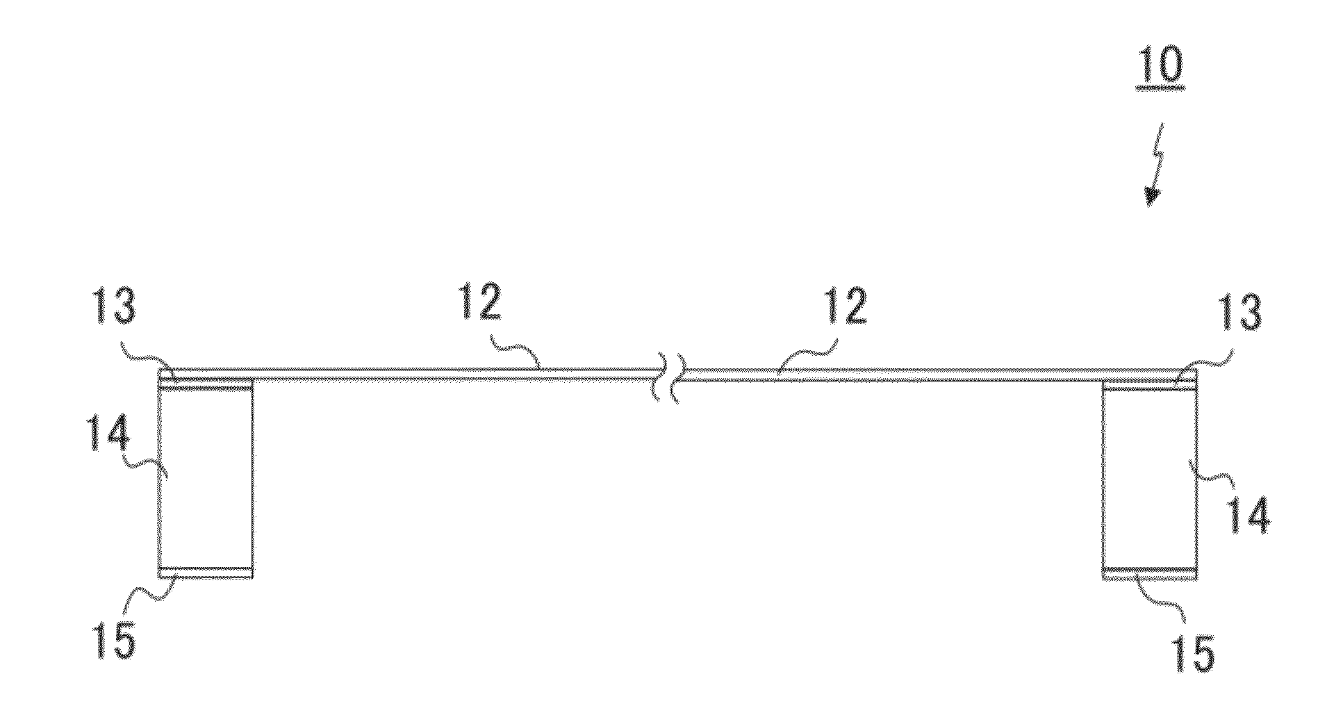
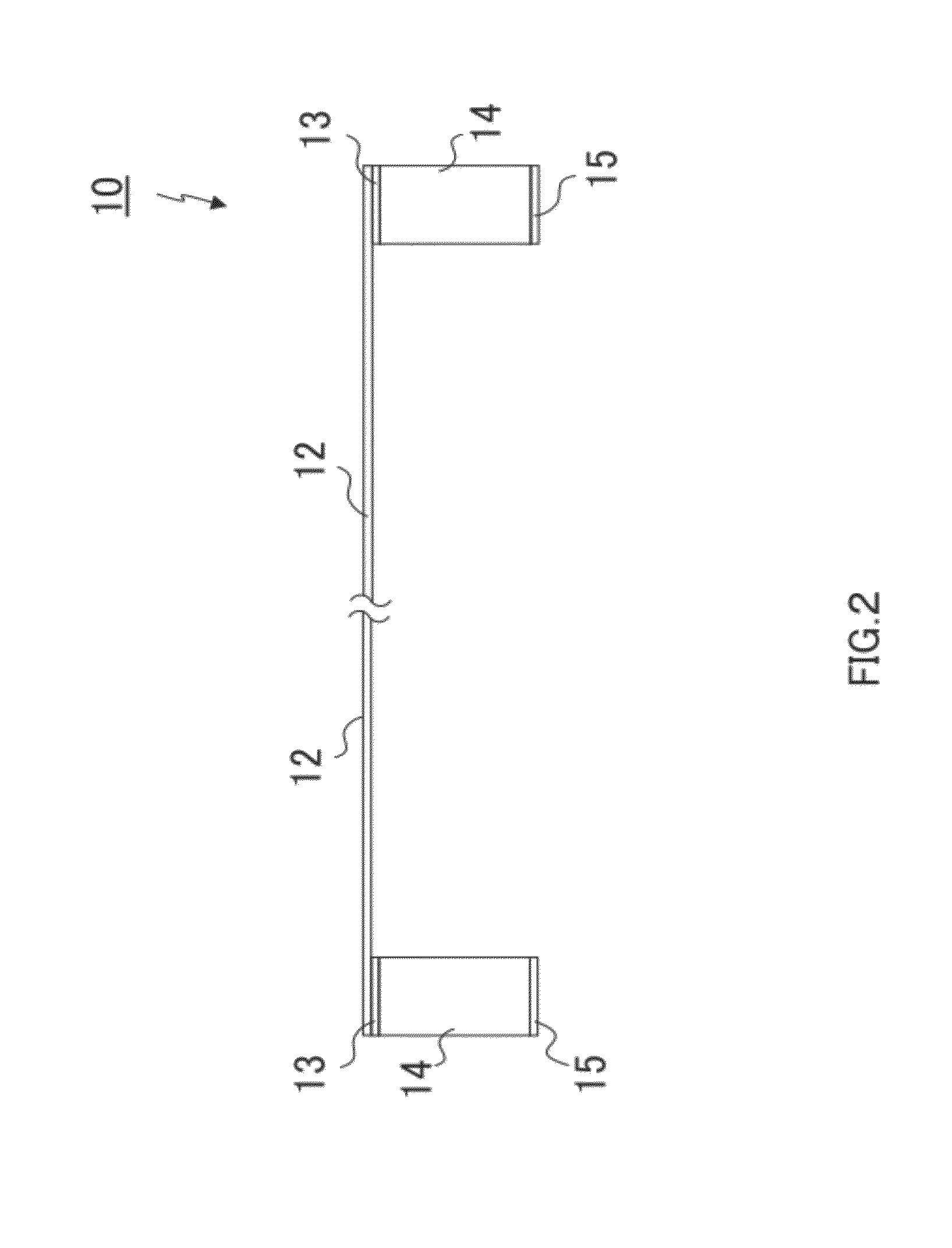
[0103]As a pellicle frame, an aluminum alloy A7075 frame (outer size: 149 mm×122 mm×5.8 mm, frame thickness: 2 mm) is provided. The surface of the pellicle frame is washed, followed by sand blast treatment at a discharge pressure of 1.5 kg / cm2.
[0104]A 10 μm-thick electrodeposited coating is formed on the pellicle frame surface using epoxy resin-based electrodeposition paint Power Top U-CP70 (Nippon Paint Co., Ltd., black matte paint). With the pellicle frame fixed at three points in an electrodeposition chamber, electrodeposition coating is carried out at a coating solution temperature of 28° C. and at impressed voltage of 200V for energization time of 90 seconds. Because electrodeposited coating thickness is subjected to change due to voltage, energization time and degradation level of the electrodeposition coating solution, an optimal coating condition for the coating thickness is determined previously.
[0105]The electrodeposited coating is then heated in a 200° C. oven for 60 minu...
example 2
[0106]A 10 μm-thick electrodeposited coating is formed on the pellicle frame surface as in Example 1 except that epoxy resin-based electrodeposition paint Power Top U-CP70-1 (Nippon Paint Co., Ltd.) is used as electrodeposition paint. A cured electrodeposited coating is formed while changing the thermal curing condition in Example 1 as follows: the electrodeposited coating is heated in a 220° C. oven for curing and drying for 60 minutes, and in aiming to reduce gas generation, it is heated in a 220° C. oven for a further 30 minutes.
example 3
[0107]As a pellicle frame, an aluminum alloy A6061 frame (outer size: 149 mm×122 mm×5.8 mm, frame thickness: 2 mm) is provided. The surface of the pellicle frame is washed, followed by sand blast treatment at a discharge pressure of 1.5 kg / cm2.
[0108]A 10 μm-thick electrodeposited coating is formed on the pellicle frame surface using epoxy resin-based electrodeposition paint Power Top U-CP70-5 (Nippon Paint Co., Ltd.). With the pellicle frame fixed at three points in an electrodeposition chamber, electrodeposition coating is carried out at a coating solution temperature of 28° C. and at impressed voltage of 200V for energization time of 80 seconds. Because electrodeposited coating thickness is subjected to change due to impressed voltage, energization time and degradation level of the electrodeposition coating solution, an optimal coating condition for the coating thickness is determined previously.
[0109]The electrodeposited coating is then heated in a 200° C. oven for 60 minutes for...
PUM
| Property | Measurement | Unit |
|---|---|---|
| thickness | aaaaa | aaaaa |
| wavelength | aaaaa | aaaaa |
| surface roughness | aaaaa | aaaaa |
Abstract
Description
Claims
Application Information