

Electronic component and method for manufacturing electronic component
- Summary
- Abstract
- Description
- Claims
- Application Information
AI Technical Summary
Benefits of technology
Problems solved by technology
Method used
Image

Examples
first preferred embodiment
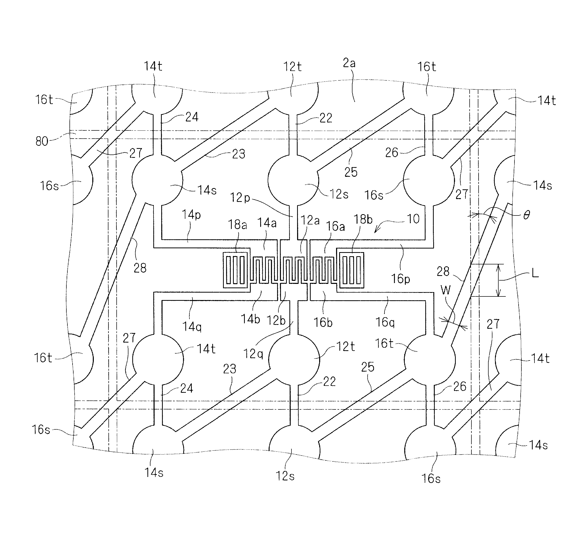
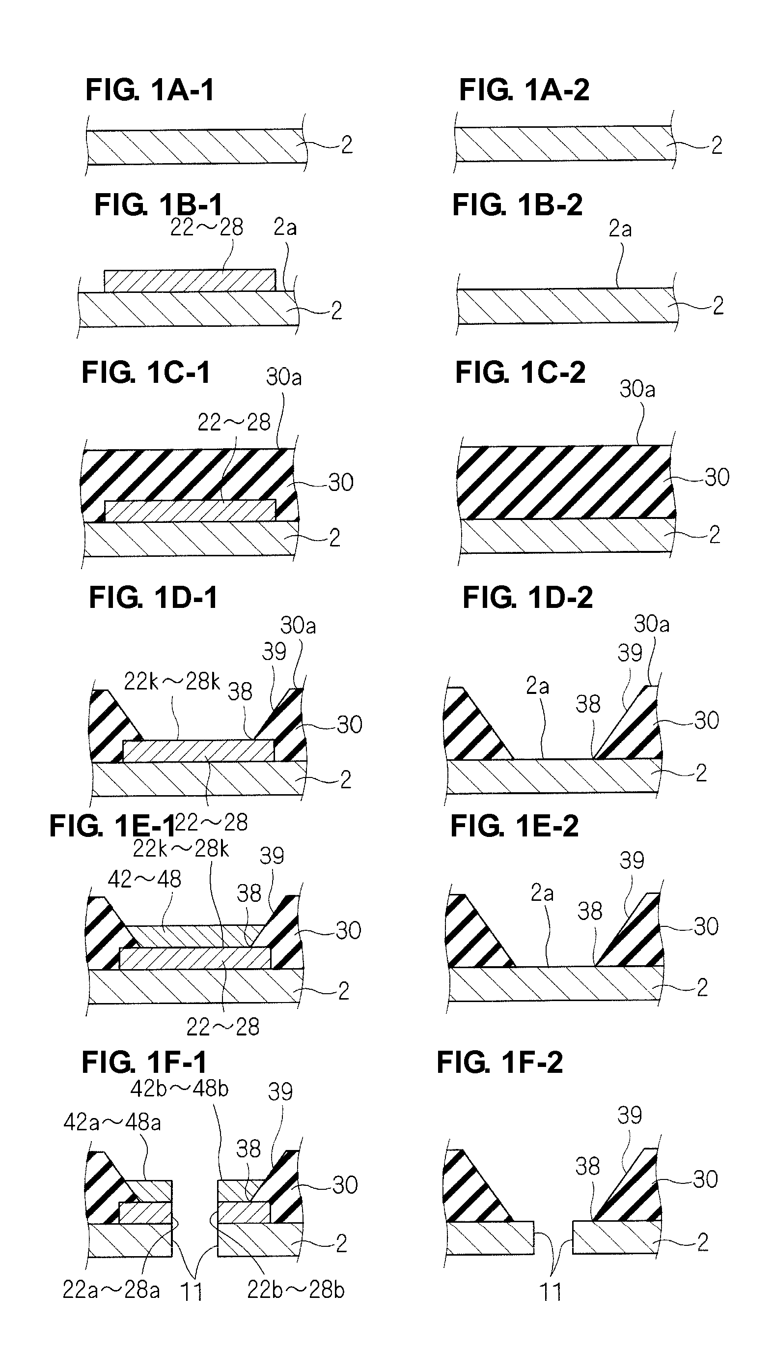
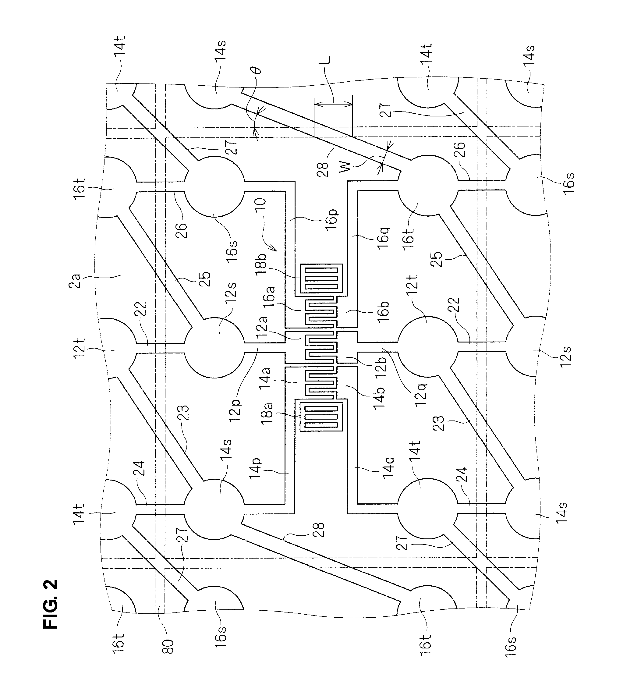
[0082]A method for manufacturing an elastic wave apparatus according to a first preferred embodiment of the present invention is described below with reference to FIGS. 1A-1 to 6. FIGS. 1A-1 to 1F-2 are cross-sectional views of a main portion of an elastic wave apparatus illustrating manufacturing steps of the elastic wave apparatus. Cross-sectional views of a main portion on the left side schematically illustrate a portion of a dicing area in which a power supply line is formed, whereas cross-sectional views of a main portion on the right side schematically illustrate a portion of the dicing area in which a power supply line is not formed. FIGS. 2 to 5 are plan views illustrating manufacturing steps of the elastic wave apparatus.
[0083]The elastic wave apparatus preferably includes an elastic wave device, such as a surface acoustic wave device or a boundary elastic wave device, for example. The elastic wave device is formed by producing a mother substrate including several elastic w...
second preferred embodiment
[0105]A method for manufacturing an elastic wave device according to a second preferred embodiment of the present invention is described below with reference to FIGS. 7A-1 to 9. FIGS. 7A-1 to 7C-2 are cross-sectional views of a main portion of an elastic wave apparatus illustrating steps of manufacturing the elastic wave apparatus. Cross-sectional views of a main portion on the left side schematically illustrate a portion of a dicing area in which a power supply line is formed, whereas cross-sectional views of a main portion on the right side schematically illustrate a portion of the dicing area in which a power supply line is not formed. FIGS. 8 and 9 are plan views illustrating manufacturing steps of the elastic wave apparatus.
[0106]The method for manufacturing an elastic wave apparatus according to a second preferred embodiment preferably is similar to the method for manufacturing an elastic wave apparatus according to the first preferred embodiment except that a conductive layer...
third preferred embodiment
[0119]A method for manufacturing an elastic wave device according to a third preferred embodiment of the present invention is described below with reference to FIGS. 10A-1 to 17. FIGS. 10A-1 to 12I′-2 are cross-sectional views of a main portion of an elastic wave apparatus illustrating steps of manufacturing the elastic wave apparatus. Cross-sectional views of a main portion on the left side schematically illustrate a portion of a dicing area in which a power supply line is formed, whereas cross-sectional views of a main portion on the right side schematically illustrate a portion of the dicing area in which a power supply line is not formed. FIGS. 13 to 17 are plan views illustrating manufacturing steps of the elastic wave apparatus.
[0120]The method for manufacturing an elastic wave apparatus according to a third preferred embodiment is substantially the same as the method for manufacturing an elastic wave apparatus according to the first or second preferred embodiments. In the fol...
PUM
| Property | Measurement | Unit |
|---|---|---|
| Angle | aaaaa | aaaaa |
| Angle | aaaaa | aaaaa |
| Power | aaaaa | aaaaa |
Abstract
Description
Claims
Application Information