Multilayer semiconductor devices with channel patterns having a graded grain structure

Active Publication Date: 2011-08-04
SAMSUNG ELECTRONICS CO LTD
View PDF6 Cites 26 Cited by
  • Summary
  • Abstract
  • Description
  • Claims
  • Application Information

AI Technical Summary

Benefits of technology

[0005]Some embodiments of the inventive subject matter provide memory devices including a stack of interleaved conductive patterns and insulating patterns disposed on a substrate and a semiconductor pattern passing through the stack of conductive patterns and insulating patterns to contact the substrate. The semiconductor pattern has a graded grain size distribution wherein a mean grain size in a f

Problems solved by technology

Therefore, integration of the device may be limited by the ability to form fin

Method used


Image

  • Multilayer semiconductor devices with channel patterns having a graded grain structure
  • Multilayer semiconductor devices with channel patterns having a graded grain structure
  • Multilayer semiconductor devices with channel patterns having a graded grain structure

Examples


Embodiment Construction

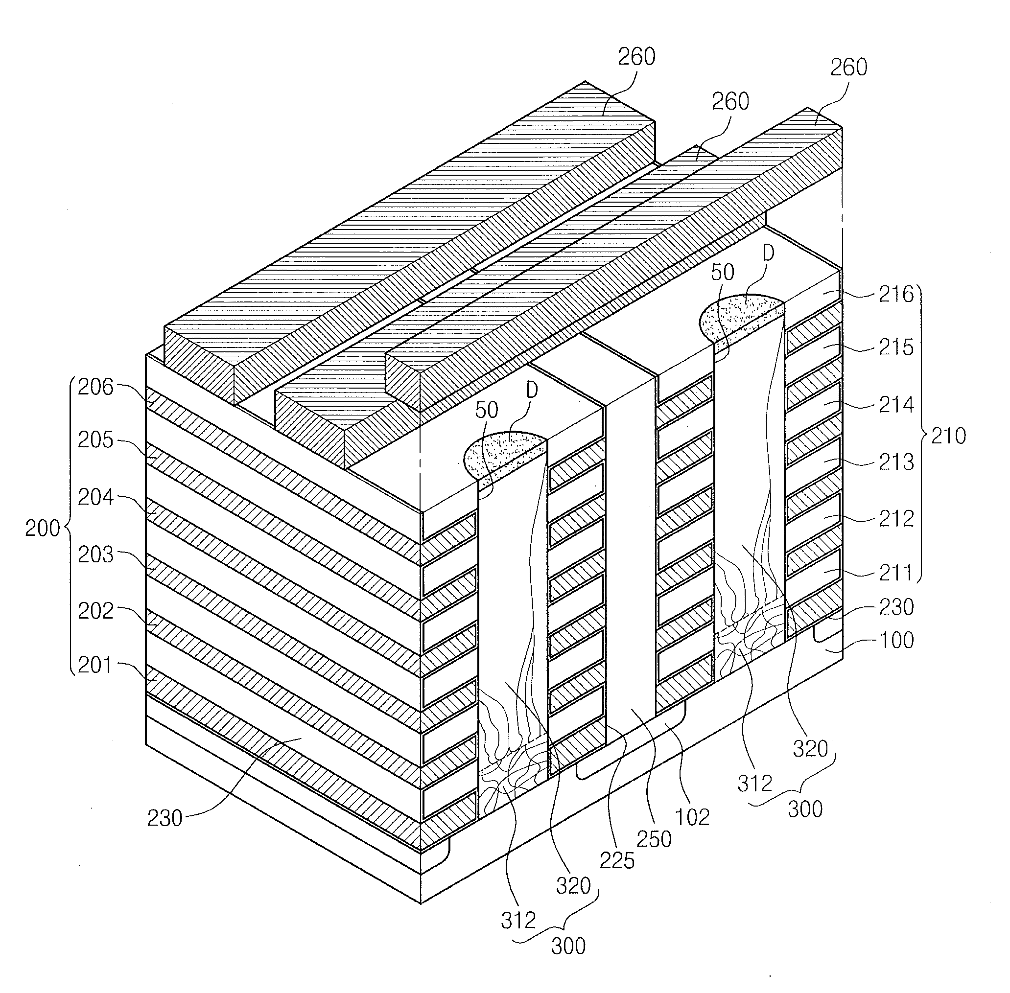
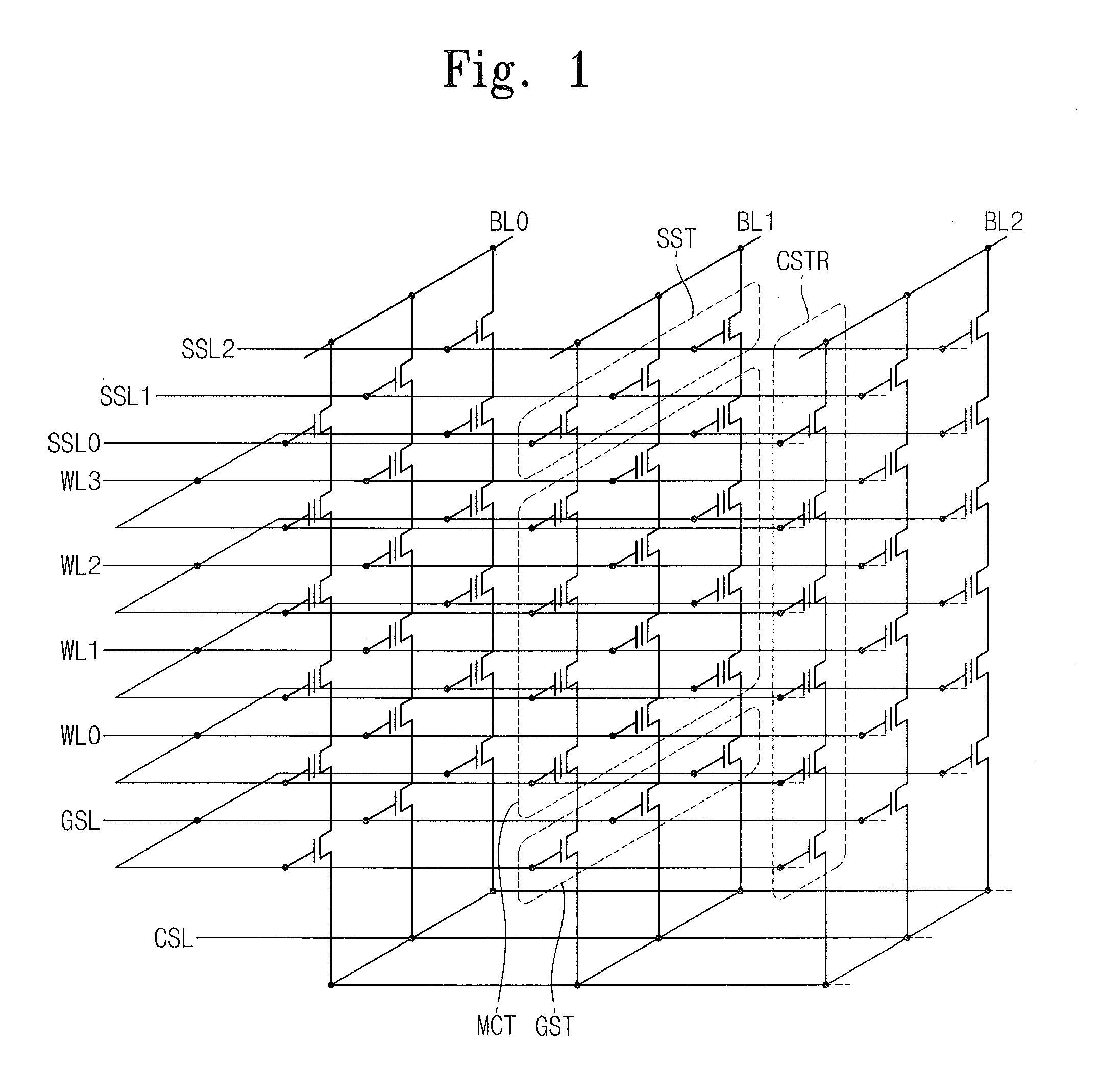
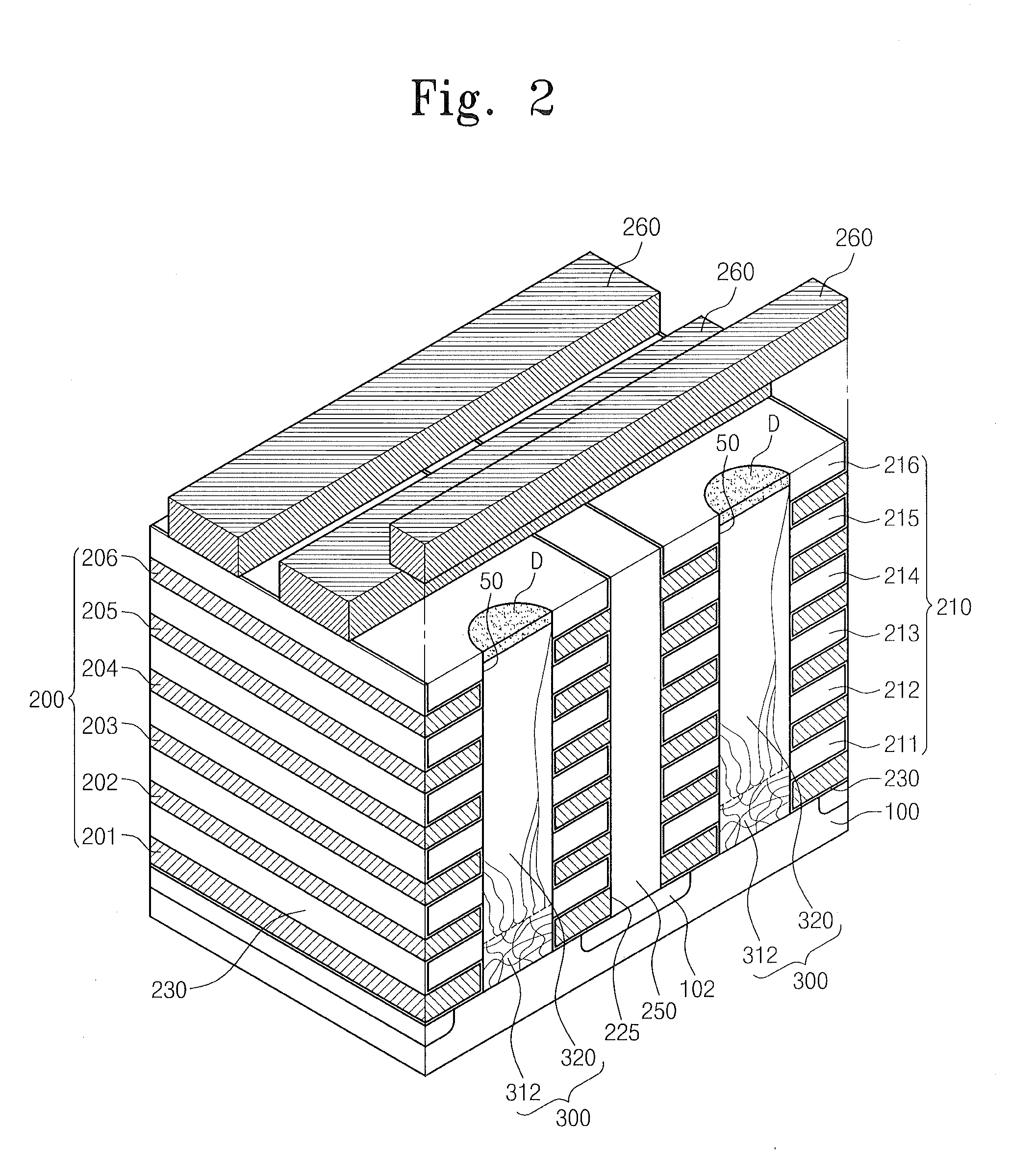
[0021]Some embodiments of the inventive subject matter will be described below in more detail with reference to the accompanying drawings. The embodiments of the inventive subject matter may, however, be embodied in different forms and should not be constructed as limited to the embodiments set forth herein. Rather, these embodiments are provided so that this disclosure will be thorough and complete, and will fully convey the scope of the inventive subject matter to those skilled in the art. Like numbers refer to like elements throughout.

[0022]The terminology used herein is for the purpose of describing particular embodiments only and is not intended to be limiting of the invention. As used herein, the singular forms “a”, “an” and “the” are intended to include the plural forms as well, unless the context clearly indicates otherwise. It will be further understood that the terms “comprises” and / or “comprising,” or “includes” and / or “including” when used in this specification, specify ...


PUM


Abstract

Memory devices include a stack of interleaved conductive patterns and insulating patterns disposed on a substrate. A semiconductor pattern passes through the stack of conductive patterns and insulating patterns to contact the substrate, the semiconductor pattern having a graded grain size distribution wherein a mean grain size in a first portion of the semiconductor pattern proximate the substrate is less than a mean grain size in a second portion of the semiconductor pattern further removed from the substrate. The graded grain size distribution may be achieved, for example, by partial laser annealing.

Description

CROSS-REFERENCE TO RELATED APPLICATIONS[0001]This U.S. non-provisional patent application claims priority under 35 U.S.C. §119 of Korean Patent Application No. 10-2010-0009628, filed on Feb. 2, 2010, the entire contents of which are hereby incorporated by reference.BACKGROUND OF THE INVENTION[0002]The present disclosure herein relates to memory devices and methods of fabrication therefore and, more particularly, to multilayer memory devices and methods of fabrication therefor.[0003]The degree of integration of semiconductor memory devices has continued to increase to meet user demands for superior performance and low price. In conventional planar (“two dimensional”) semiconductor memory devices, the degree of integration is generally determined by the area which a unit memory cell occupies. Therefore, integration of the device may be limited by the ability to form fine patterns. Producing finer patterns may require expensive production equipment.[0004]“Three dimensional” (multilayer...

Claims


Application Information

Patent Timeline
IPC IPC(8): H01L29/04H01L21/20
CPCH01L29/04H01L21/20H10B43/27H01L27/0688H10B43/20
Inventor SON, YONG-HOONLEE, MYOUNGBUMHWANG, KIHYUN
Owner SAMSUNG ELECTRONICS CO LTD
Why Eureka
Try Eureka