Electrostatic discharge protection circuit

a protection circuit and electrostatic discharge technology, applied in semiconductor devices, semiconductor/solid-state device details, transistors, etc., can solve the problems of damage to the internal circuit, damage to the integrated circuit, etc., and achieve the effect of efficient cdm esd protection performan

Active Publication Date: 2011-08-18
UNITED MICROELECTRONICS CORP +1
View PDF12 Cites 14 Cited by
  • Summary
  • Abstract
  • Description
  • Claims
  • Application Information

AI Technical Summary

Benefits of technology

[0019]As described above, in the present application, a circuit formed by a PMOS transistor and a resistor serves as a CDM ESD protection circuit. The ESD protection circuit has an initial-on mechanism by connecting a gate of the PMOS transistor to a power rail through the resistor so that the turn-on speed of the ESD protection circuit is enhanced and efficient CDM ESD protection performance is achieved.

Problems solved by technology

ICs are generally susceptible to ESD events, which may damage or destroy the integrated circuit.
Since the duration of CDM ESD events is much shorter than HBM and MM ESD events, the internal circuit may be damaged during CDM ESD events before the ESD protection circuit is turned on.

Method used


Image

  • Electrostatic discharge protection circuit
  • Electrostatic discharge protection circuit
  • Electrostatic discharge protection circuit

Examples


first embodiment

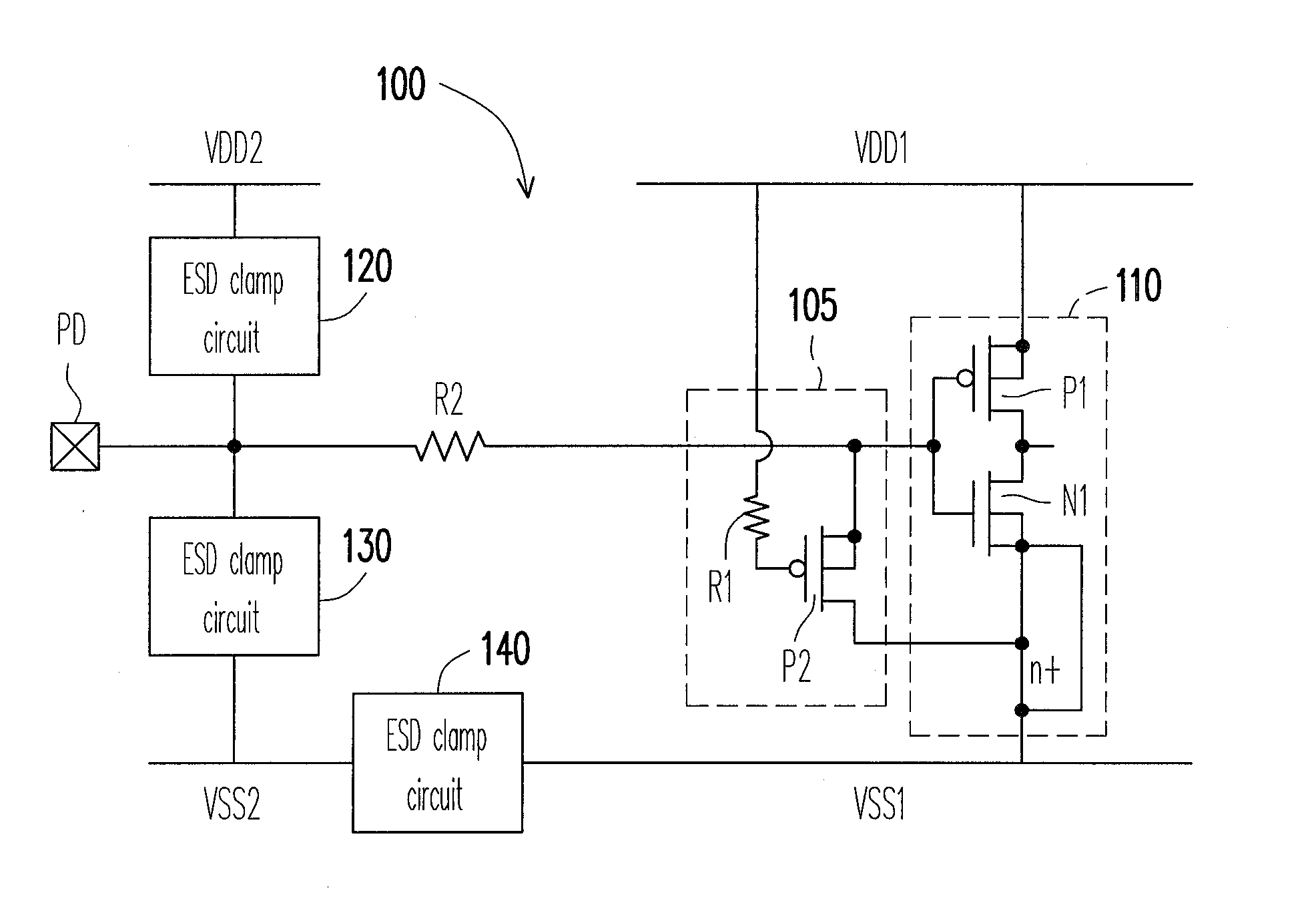
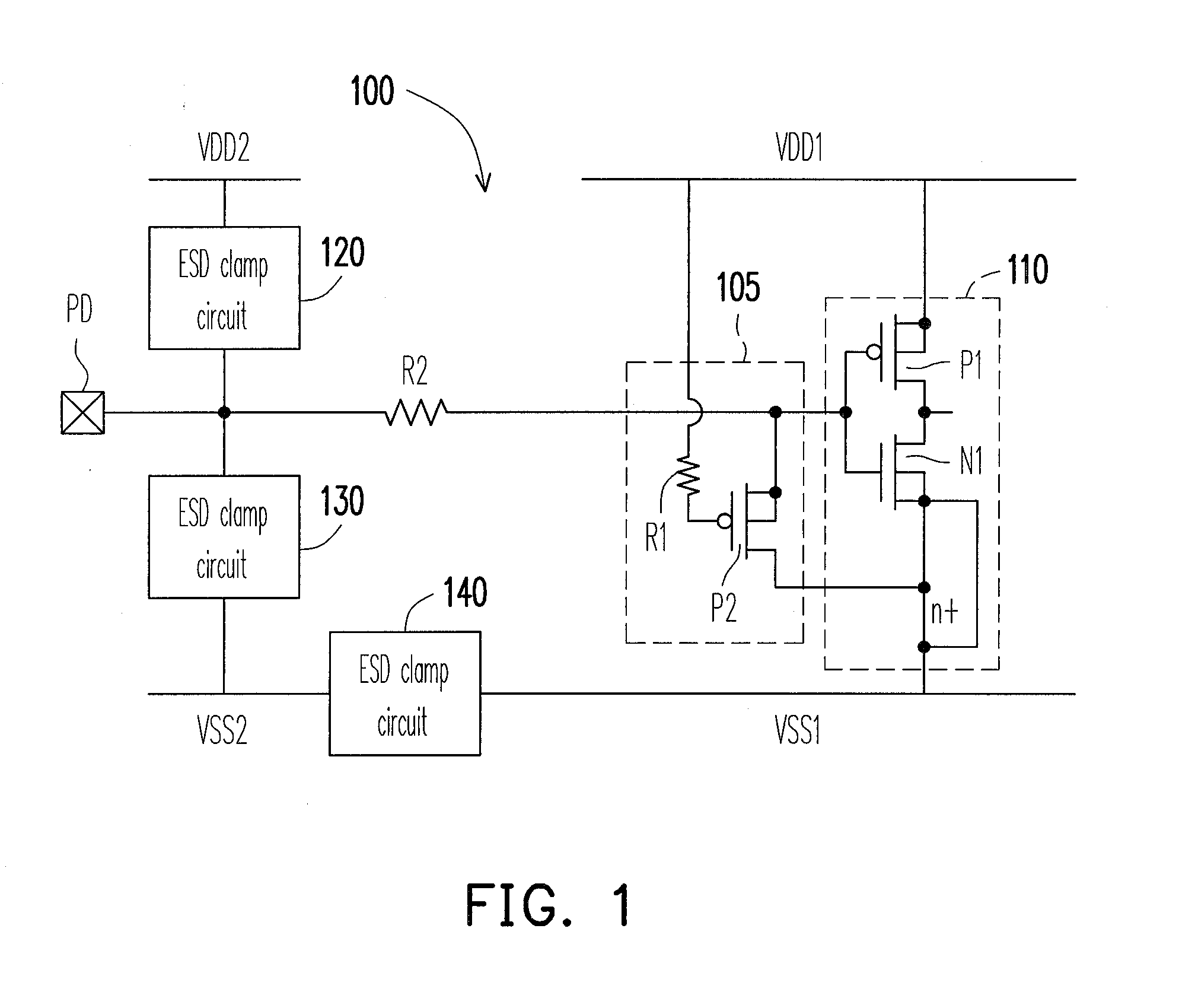
[0031]FIG. 1 shows a circuit diagram capable of ESD protection in accordance with a first embodiment of the application. Referring to FIG. 1, a circuit 100 includes an input stage circuit 110, a PMOS transistor P2, two resistors R1 and R2, and ESD clamp circuits 120, 130 and 140, wherein the input stage circuit 110 further includes a first PMOS transistor P1 and a first NMOS transistor N1. The first PMOS transistor P1 has a source and a body both coupled to a first power rail VDD1, and a drain coupled to a drain of the first NMOS transistor N1. The first NMOS transistor N1 has a source and a body both coupled to a first ground rail VSS1, and a gate coupled to a gate of the first PMOS transistor P1. The resistor R2 is coupled between the gate of the first PMOS transistor P1 and an input pad PD. It is noted that the resistor R2 is not necessary in the circuit 100, the input stage circuit 110 can directly connect to the input pad PD without the resistor R2.

[0032]The ESD clamp circuit 1...

second embodiment

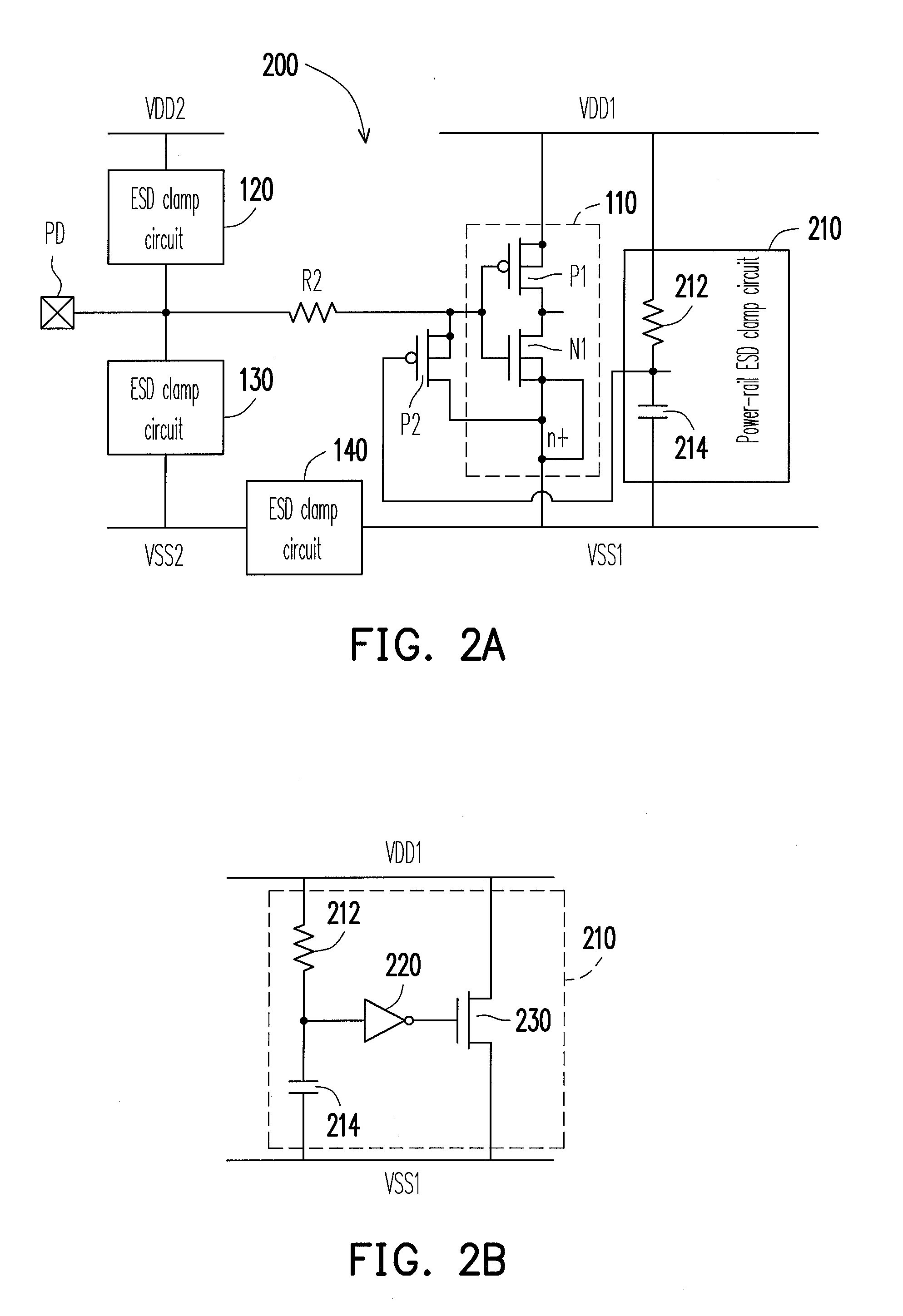
[0034]The resistor R1 of FIG. 1 can be replaced with a resistor of a power-rail ESD clamp circuit. FIG. 2A shows a circuit diagram capable of ESD protection in accordance with a second embodiment of the application. Referring to FIG. 2A and FIG. 1, the difference between a circuit 200 and the circuit 100 is mainly a power-rail ESD clamp circuit 210, as shown in FIG. 2A. The power-rail ESD clamp circuit 210 is coupled between the first power rail VDD1 and the first ground rail VSS1, and capable of providing ESD protection for the first power rail VDD1 and the first ground rail VSS1. The power-rail ESD clamp circuit 210 includes a resistor 212 and a capacitor 214, in which the resistor 212 and a capacitor 214 are connected in series between the first power rail VDD1 and the first ground rail VSS1. The gate of the PMOS transistor P2 is coupled to a common node of the resistor 212 and the capacitor 214, and therefore coupled to the first power rail VDD1 through the resistor 212.

[0035]Th...

third embodiment

[0036]According to another embodiment of the present application, the ESD protection designs can be implemented by an additional PMOS circuit in conjunction with a source loading (for example, resistor, diode, or MOS), as shown in FIGS. 3-6. Referring to FIG. 3, FIG. 3 shows a circuit 300 capable of ESD protection in accordance with the third embodiment of the application. The difference between the circuit 300 and circuit 100 as shown in FIG. 1 is mainly a diode 310, the diode 310 has a anode coupled to the source of the first NMOS transistor N1, and a cathode coupled to the first ground rail VSS1. Similarly, the diode 310 can also be added to the circuit 200 as shown in FIG. 2A. Referring to FIG. 4, FIG. 4 shows another circuit 400 capable of ESD protection in accordance with the third embodiment of the application. The circuit 400 includes the diode 310 and the power-rail clamp circuit 210, wherein the diode 310 is coupled between the first NMOS N1 and the first ground rail VSS1....


PUM


Abstract

An electrostatic discharge (ESD) protection circuit, suitable for an input stage circuit including a first N channel metal oxide semiconductor (NMOS) transistor, is provided. The ESD protection circuit includes an P channel metal oxide semiconductor (PMOS) transistor and an impedance device, in which the PMOS transistor has a source coupled to a gate of the first NMOS transistor, and a drain coupled to a source of the first NMOS transistor, and the impedance device is coupled between a gate of the PMOS transistor and a first power rail to perform a initial-on ESD protection circuit. The ESD protection circuit formed by the PMOS transistor and the resistor is capable of increasing the turn-on speed of the ESD protection circuit and preventing the input stage circuit from a CDM ESD event.

Description

BACKGROUND OF THE INVENTION[0001]1. Field of the Invention[0002]The present invention generally relates to an electrostatic discharge (ESD) protection circuit, in particular, to a Charged-Device Model (CDM) ESD protection circuit.[0003]2. Description of Related Art[0004]An ESD event refers to a phenomenon of electrical discharge of a current for a short duration during which a large amount of current is provided to a semiconductor integrated circuit (IC). ICs are generally susceptible to ESD events, which may damage or destroy the integrated circuit. Thus, ESD protection of ICs is a critical factor in obtaining high yield and stable IC characteristics. The susceptibility of a device to ESD can be determined by testing each one of three models which include Human Body Model (HBM), Machines Model (MM) and Charged-Device Model (CDM).[0005]With regard to a CDM ESD event, electrostatic charge could be stored within the body of an IC product due to induction or tribocharging and most of t...

Claims


Application Information

Patent Timeline
Patent Type & Authority Applications(United States)
IPC IPC(8): H01L27/06H01L23/60
CPCH02H9/046H01L27/0285
Inventor KER, MING-DOULIN, CHUN-YUWANG, CHANG-TZU
Owner UNITED MICROELECTRONICS CORP
Why Eureka
Try Eureka