Flotox-based, bit-alterable, combo flash and eeprom memory

Inactive Publication Date: 2011-08-18
APLUS FLASH TECH
View PDF2 Cites 14 Cited by
  • Summary
  • Abstract
  • Description
  • Claims
  • Application Information

AI Technical Summary

Benefits of technology

[0039]The present invention discloses a novel array circuit architecture for 1T FLOTOX-based flash and 2T FLOTOX-based EEPROM arrays along with a respective set of preferred biased voltage conditions for BL, SL, FGBL, SWL and FWL to greatly reduce the punch-through leakage flowing through the unselected EEPROM or flash cells. In addition, the present invention provides both 1T FLOTOX-based flash and 2T FLOTOX-based EEPROM arrays with a bit-alterable write function. With the added bit-alterable write function, the elimination of unnecessary 16.0V HV stress on the thin tunneling oxide gate layer of the memory cells can be achieved for a superior endurance cycles and thus a longer product life.
[0043]It is another object of the present invention to provide a preferred program method of the novel 2T FLOTOX-based EEPROM array. Unlike the traditional byte-program method, the present invention allows the Vt to decrease only on the selected 2T FLOTOX-based EEPROM cells by using novel reverse FN bit-program biased conditions in accordance with a preferable operation.
[0044]A further object of the present invention is to provide a set of preferred biased program conditions for BLs and SLs of the novel 2T FLOTOX-based EEPROM array to reduce the HV drop across the channel region between the drain node and source node of the double-poly FTb transistor of each FT in the novel 2T FLOTOX-based EEPROM array of the present invention.
[0048]Another object of the present invention is to provide a novel 1T FLOTOX-based flash array in which the number of source lines is made identical to the number of bit lines. Each bit line is connected to the drains of all the associated FT transistors organized in a vertical column of the novel 1T FLOTOX-based flash array in the present invention and the corresponding source line is connected to the common sources of all the FT transistors in the vertical column. Both bit lines and source lines are preferably made in parallel and laid out vertically in silicon as a plurality of metal lines perpendicular to all horizontal word lines to reduce area for superior cell scalability.
[0050]It is another object of the present invention to provide a preferred program method of the novel 1T FLOTOX-based flash array. Unlike the traditional byte-program method, the present invention allows the Vt to decrease only on the selected 1T FLOTOX-based flash cells by using novel reverse FN bit-program biased conditions in accordance with a preferred operation.
[0051]A further object of the present invention is to provide a set of preferred biased program conditions for BLs and SLs of the novel 1T FLOTOX-based flash array to reduce the HV drop across the channel region between the drain node and source node of the double-poly FTb transistor of each FT in the novel 1T FLOTOX-based flash array of the present invention.

Problems solved by technology

As a result, 16.0V cannot be sustained within the channel regions of the four FTa devices in FT0, FT2, FT4 and FT6, and the desired program operation would fail.
Therefore, the channel lengths of all FTb devices have to be kept larger to avoid the punch-through effect, and thus the cell size of the EEPROM array is large and difficult to scale below 0.13 um technology.
Because the HV is supplied from a weak source, any leakage along the selected path would result in the voltage drop across the tunnel-oxide of the selected cells, thus the FN byte-program would fail.
This leakage is due to the occurrence of the channel punch-through of unselected ST devices connected to each BL.
The drawback of unnecessary HV (16V) over stress on the thin tunnel-oxide gate of EEPROM cells is partly due to the unique byte-alterable array architecture with a shared horizontal source line of the selected byte in the conventional FLOTOX-based 2T EEPROM array.
As a result, the EEPROM program operation would fail.
The unsuccessful program operation in the byte-alterable FLOTOX-based EEPROM array can easily happen when the channel lengths of FTb and ST are reduced.
As a consequence, the scalability of the cell size has encountered a big bottleneck in the traditional EEPROM design.

Method used


Image

  • Flotox-based, bit-alterable, combo flash and eeprom memory
  • Flotox-based, bit-alterable, combo flash and eeprom memory
  • Flotox-based, bit-alterable, combo flash and eeprom memory

Examples


Embodiment Construction

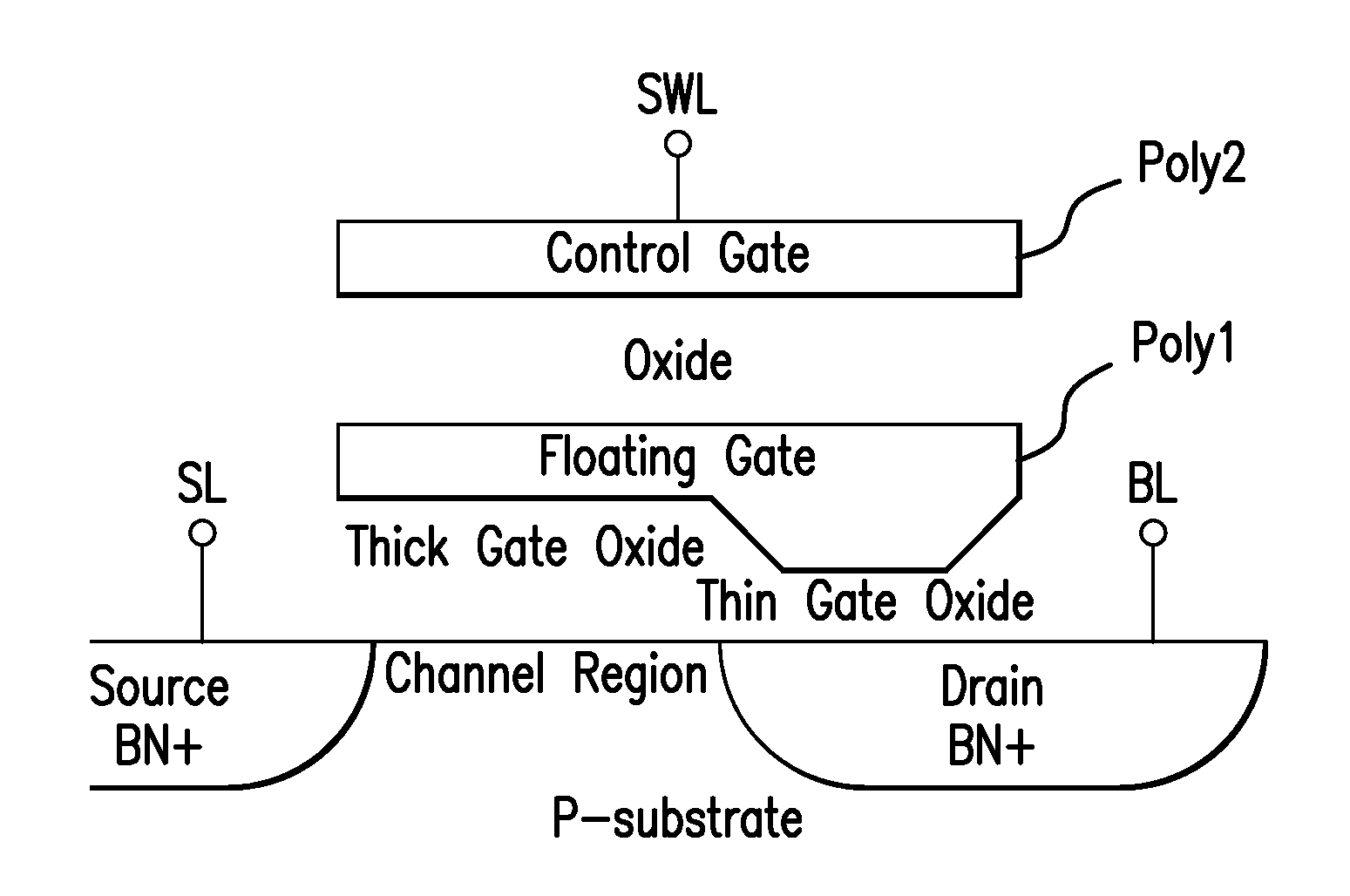
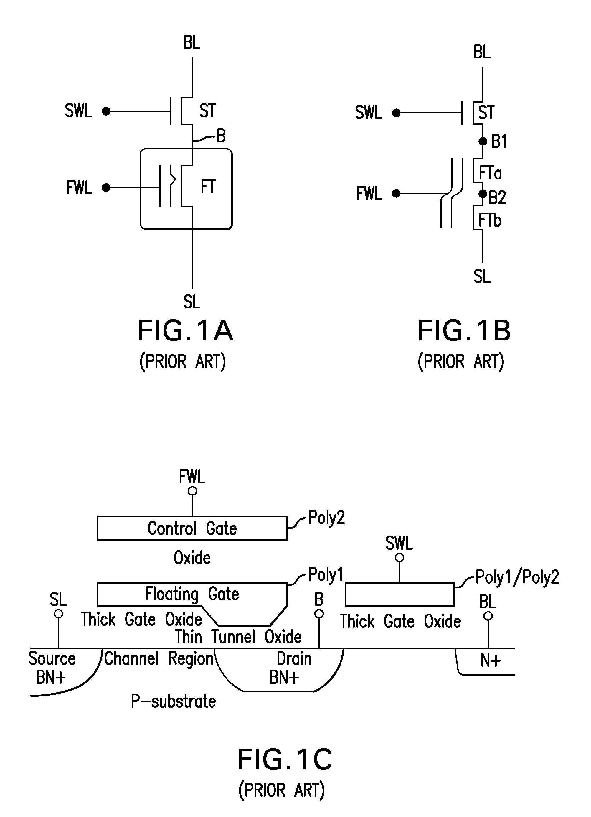
[0072]With reference to FIGS. 2A-2C, the present invention provides a novel 2T FLOTOX-based EEPROM cell array which is both byte-alterable and bit-alterable. As shown in FIGS. 2A and 2B, the basic 2T FLOTOX-based EEPROM cell structure in the EEPROM cell array shown in FIG. 2C is identical to the conventional 2T FLOTOX-based EEPROM cell structure shown in FIGS. 1A and 1B. The detailed description for the EEPROM cell structure and its operation principle has been given in Background of the Invention, and therefore will not be repeated here. As mentioned in the description for FIG. 1A, SL is always connected to VSS in the traditional EEPROM array. However, SL shown in FIG. 2A is connected to a preferred read, program or erasure voltage respectively through a source line decoder in accordance with the present invention.

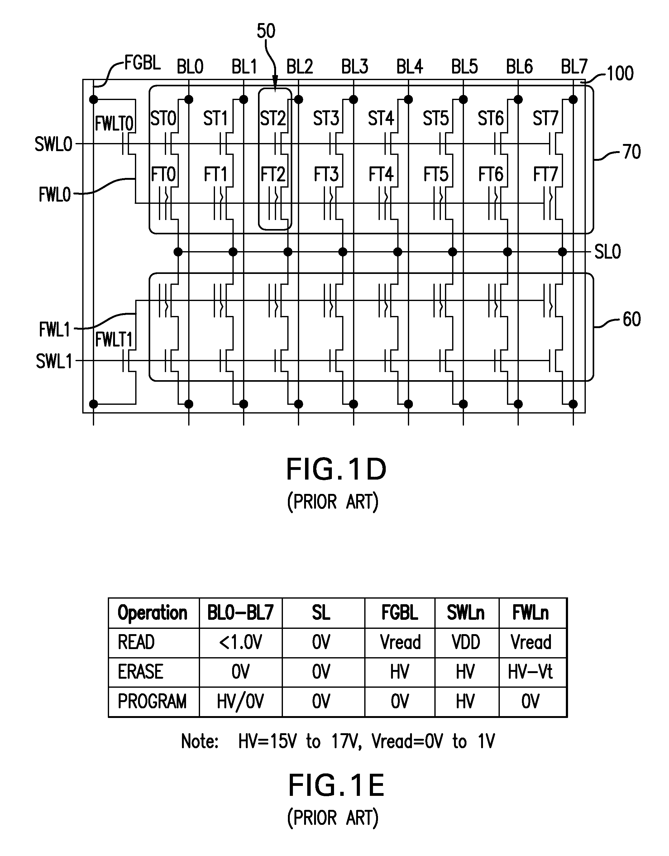
[0073]FIG. 2C shows an exemplary circuit of a 2T FLOTOX-based EEPROM cell array 400 according to the present invention for byte-alterable and bit-alterable code storage. ...


PUM


Abstract

A non-volatile memory array having FLOTOX-based memory cells connected by a plurality of word lines and a plurality of bit lines is disclosed. In the memory array, the FLOTOX-based memory cells in a common word line do not share a common source line. Instead, the FLOTOX-based memory cells associated with a bit line are provided with a source line laid out in parallel with the bit line to avoid punch-through leakage. The FLOTOX-based memory cells may be 2T FLOTOX-based EEPROM cells or 1T FLOTOX-based flash cells. The byte-alterable and page-alterable functions of a 2T EEPROM array and the block-alterable function of a 1T flash array are preserved. In addition, a novel bit-alterable function is added to both 2T FLOTOX-based EEPROM array and 1T FLOTOX-based flash array to reduce the unnecessary high voltage over-stress in a write operation to improve program / erasure endurance cycles.

Description

CROSS-REFERENCE TO RELATED APPLICATIONS[0001]This application claims priority under 35 U.S.C. §119 to U.S. Provisional Patent Application Ser. No. 61 / 337,991, filed on Feb. 12, 2010, assigned to the same assignee as the present invention, and incorporated herein by reference in its entirety.RELATED PATENT APPLICATIONS[0002]U.S. Provisional Patent Application Ser. No. 61 / 126,854, filed on May 7, 2008, assigned to the same assignee as the present invention, and incorporated herein by reference in its entirety.[0003]U.S. Provisional Patent Application Ser. No. 61 / 130,381, filed on May 30, 2008, assigned to the same assignee as the present invention, and incorporated herein by reference in its entirety.BACKGROUND OF THE INVENTION[0004]1. Field of the Invention[0005]This invention relates generally to nonvolatile memory circuits, devices, and methods of operation. More particularly, this invention relates to floating gate tunneling oxide based (FLOTOX-based) nonvolatile memory circuits, ...

Claims


Application Information

Patent Timeline
IPC IPC(8): G11C16/10G11C16/16
CPCG11C16/10G11C16/0433G11C11/005
Inventor LEE, PETER WUNGHSU, FU-CHANG
Owner APLUS FLASH TECH
Why Eureka
Try Eureka