High Voltage Word Line Driver

Inactive Publication Date: 2011-08-18
IBM CORP
View PDF16 Cites 61 Cited by
  • Summary
  • Abstract
  • Description
  • Claims
  • Application Information

AI Technical Summary

Benefits of technology

Principles of the invention provide a high voltage word line driver circuit for use, for example, in a DRAM array. Advantageously, embodiments of the invention provide a word line driver comprising an output d

Problems solved by technology

Unfortunately, higher voltages applied to the memory cells can damage transistors associated with these cells over time.
These reliability constraints, however, prevent conventional memory circuits from achieving the above-stated benefits of using higher word line voltages.

Method used


Image

  • High Voltage Word Line Driver
  • High Voltage Word Line Driver
  • High Voltage Word Line Driver

Examples


case 3

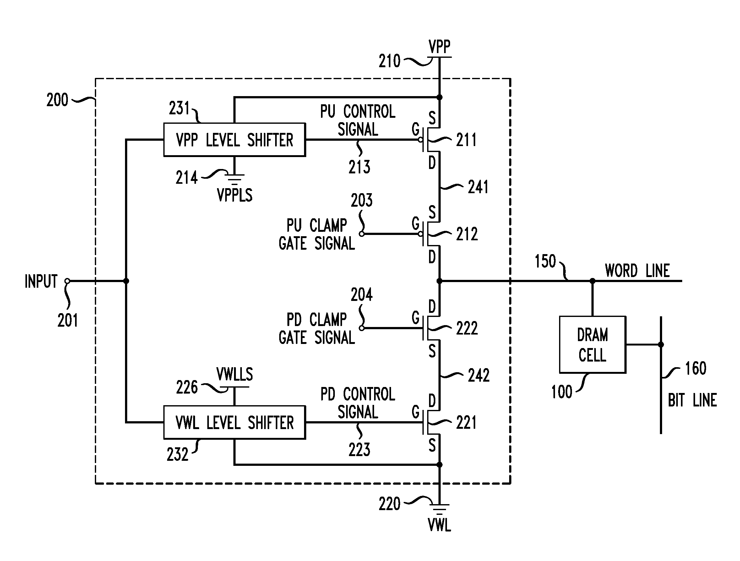
Regarding case 3, setting VPPLS, VWLLS, VPU and VPD to a common 0.7 V voltage level ensures that a magnitude (i.e., absolute value) of the gate-to-drain and gate-to-source voltages for each of the transistors 211, 212, 221 and 222 does not exceed about one-half of VPP minus one-half of VWL (e.g., VPP / 2−VWL / 2), which is about 1.05 volts in this illustrative embodiment, either when the word line 150 is driven to or maintained at high (e.g., VPP) or low (e.g., VWL) voltage levels. Note, that the gate-to-source and gate-to-drain voltages for each of the transistors 211, 212, 221 and 222 will preferably not exceed VDD (e.g., about 1.1 volts), and thus will not exceed prescribed gate-to-source or gate-to-drain voltage limits for a thin-oxide (i.e., logic) transistor.

For case 3, with two exceptions, the magnitude of the source-to-drain voltage difference for transistors 211, 212, 221 and 222 does not exceed VDD and is at most one-half of VPP minus one-half of WWL (VPP / 2−VWL / 2). The two exc...

case 2

In case 2 of Table 1, with the input 201 equal to about 0 volts, the output of the VWL level shifter 232 driving the drain of pull-down gate clamp transistor 721 will be about 1.1 volts (VDD). Transistor 721 is operative to shift the 1.1 volts received at it drain to about a threshold voltage (VT721) below the voltage of the common gate node 703. By way of example only, node 703 is preferably set to a voltage of about 0.7 volt. A voltage of about 0.7 volt for node 703 is consistent with the pull-up clamp voltage level (VPU) and pull-down clamp voltage level (VPD), which are the voltages that nodes 203 and 204, respectively, are set to in For case 2, with the input 201 equal to about 0 volts, node 703 voltage equal to about 0.7 volt, and a threshold voltage for transistor 721 of about 0.2 volt, the gate voltage of transistor 221 will be about 0.5 volt (i.e., about 0.7V−0.2V). Thus, the magnitude of the gate-to-source voltage and the magnitude of the gate-to-drain voltage for transis...


PUM


Abstract

A word line driver circuit coupled to a memory circuit word line includes pull-up, pull-up clamp, pull-down and pull-down clamp transistors, each having a source, a drain and a gate. For the pull-up transistor, the source is coupled to a first power supply, and the gate to a pull-up control signal. For the pull-up clamp transistor, the source is coupled to the drain of the pull-up transistor, the drain to the word line, and the gate to a pull-up clamp gate signal. For the pull-down transistor, the source is coupled to a second power supply, and the gate to a pull-down control signal. For the pull-down clamp transistor, the source is coupled to the drain of the pull-down transistor, the drain to the word line, and the gate to a pull-down clamp gate signal. The word line is coupled to one or more DRAM cells. Source to drain voltage magnitudes of the pull-up and pull-down transistors are less than a voltage between the first and second power supplies.

Description

FIELD OF THE INVENTIONThe present invention relates generally to the electrical, electronic, and computer arts, and more particularly relates to word line driver circuits for use in a memory device.BACKGROUND OF THE INVENTIONMemory circuits typically include a memory array comprising a plurality of memory cells coupled to an arrangement of word lines and bit lines, each memory cell being coupled to a corresponding unique word line and bit line pair. There may be a plurality of memory cells coupled to a given word line and / or a given bit line. The term “word line” as used in the context of a memory array is sometimes referred to as a “row.” Similarly, the term “bit line” in the contact of a memory array is sometimes referred to as a “column.” It is to be understood that the terms “word line” and “bit line” as used herein are intended to have the same meaning as, and may therefore be used interchangeably with, the terms “row” and “column,” respectively.A word line driver circuit is ty...

Claims


Application Information

Patent Timeline
IPC IPC(8): G11C8/08G11C7/00
CPCG11C11/4085G11C8/08
Inventor REOHR, WILLIAM ROBERTBARTH, JR., JOHN EDWARDKIRIHATA, TOSHIAKILEU, DEREK H.PLASS, DONALD W.
Owner IBM CORP
Why Eureka
Try Eureka