Organic electric field light emitting element and production therefor
a technology of light-emitting elements and organic electric fields, which is applied in the direction of luminescent compositions, thermoelectric devices, chemistry apparatuses and processes, etc., can solve the problems of difficult control of the degree of polymerization and the molecular weight distribution of high molecular weight materials, and the wet coating process is not developed to a practical level. , to achieve the effect of satisfactory operating life and excellent luminous efficiency
- Summary
- Abstract
- Description
- Claims
- Application Information
AI Technical Summary
Benefits of technology
Problems solved by technology
Method used
Image
Examples
example 1
Device Preparation 1
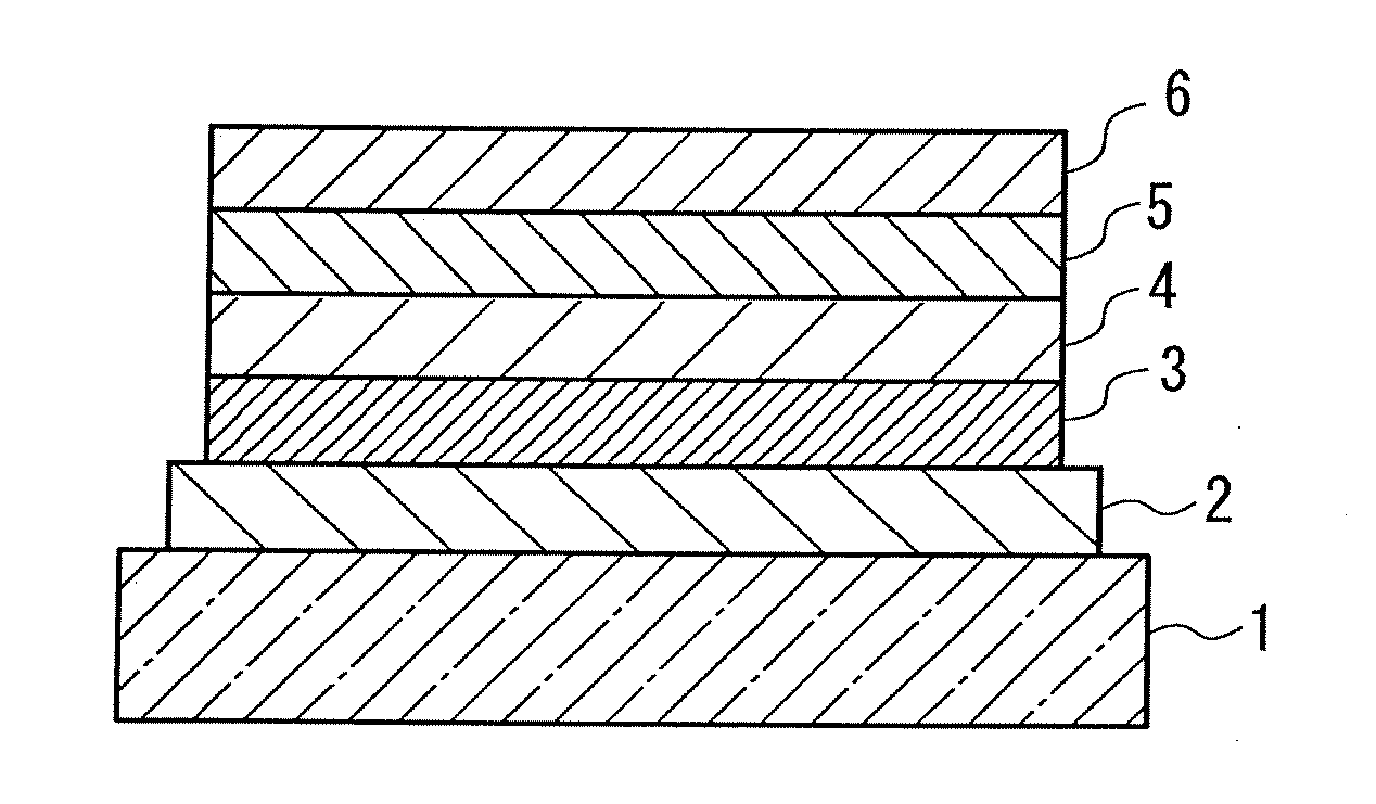
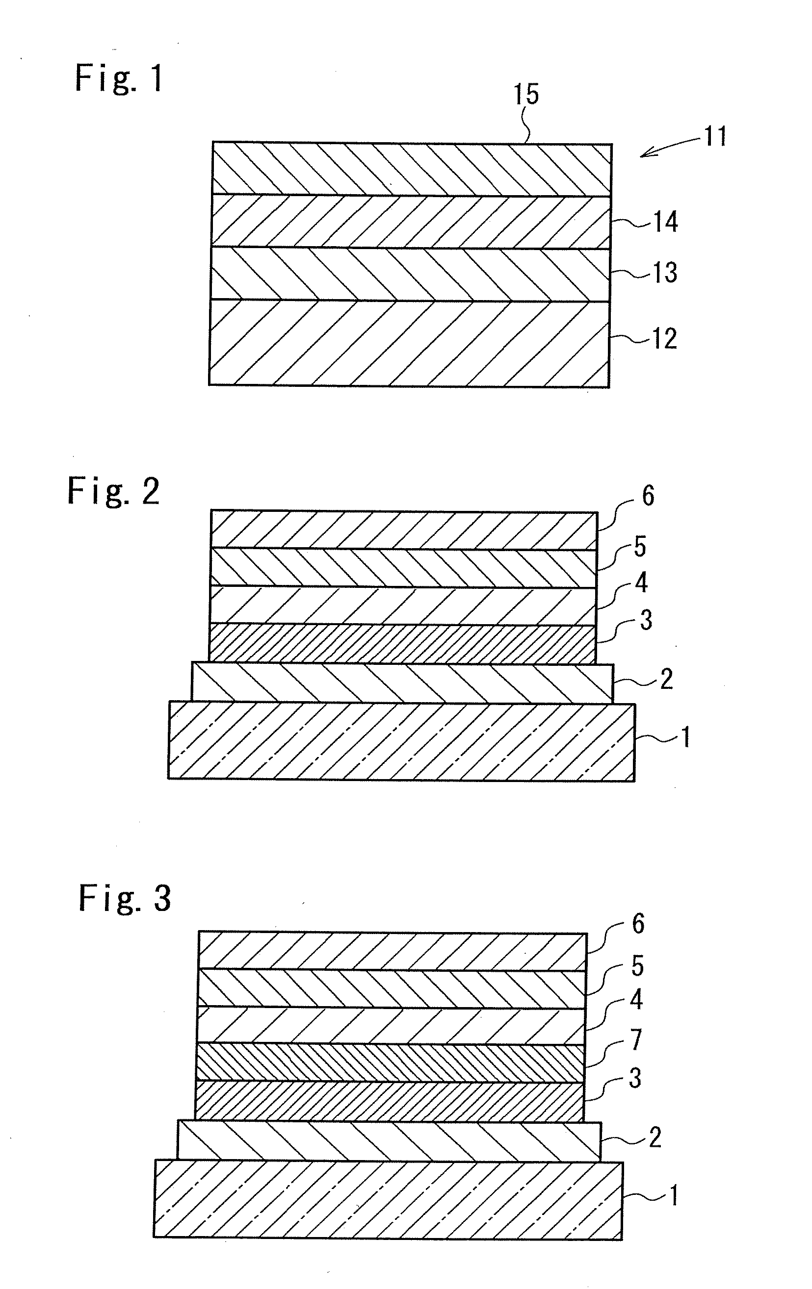
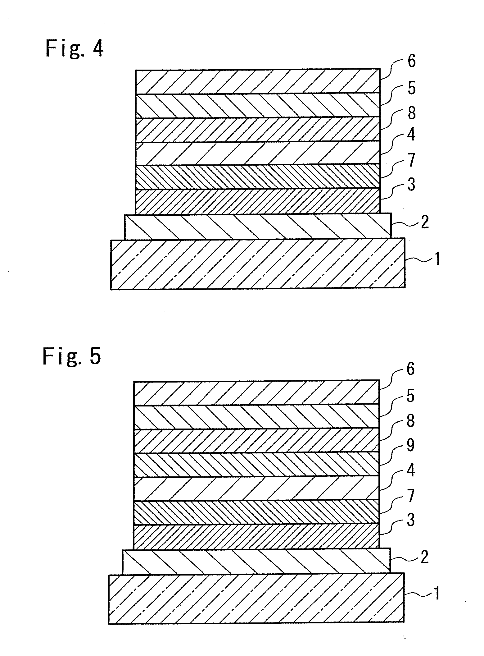
[0409]An indium-tin oxide (ITO) transparent electroconductive film deposited to a thickness of 150 nm on a glass substrate (supplied from Sanyo Vacuum Industries Co., Ltd., sputtered film) was patterned in a 2-mm width stripe pattern using a common photolithography technique and etching with hydrochloric acid-iron chloride solution thereby forming an anode. The patterned ITO substrate was rinsed by sequentially carrying out ultrasonic cleaning in an aqueous surfactant solution and rinsing with pure water, followed by drying in dried nitrogen gas, and UV / ozone cleaning. In addition, a composition for an organic electroluminescent device was prepared by mixing 90 mg of the compound (T1), 90 mg of the compound (T2), and 9 mg of the compound (D1), each represented by the structural formula, and 2.8 g of chlorobenzene as a solvent, and removing insoluble matter by filtration through a PTFE membrane filter having a pore size of 0.2 μm. The composition was applied to th...
example 2
Device Preparation 2
[0420]A composition for an organic electroluminescent device was prepared by mixing 90 mg of the compound (T3), 90 mg of the compound (T4), and 9 mg of the compound (D1), each represented by the structural formula, and 2.8 g of o-dichlorobenzene as a solvent, and removing insoluble matter by filtration through a PTFE membrane filter having a pore size of 0.2 μm. In addition, an ITO substrate was patterned and rinsed in the same manner as with Example 1. The composition was applied to the resulting ITO substrate by spin coating under the following conditions to thereby form a uniform thin film having a thickness of 160 nm.
[0421]Revolution number of spinner: 1500 rpm
[0422]Revolution time of spinner: 30 seconds
[0423]Spinning atmosphere: spinning was conducted in the atmosphere at a temperature of 23° C. and relative humidity of 30%
[0424]Drying condition: drying by heating on a hot plate at 80° C. for 1 minutes and further drying by heating in an oven at 140° C. for ...
example 3
Device Preparation 3
[0431]Initially, an ITO substrate was patterned and rinsed in the same manner as with Example 2 and was immersed in a solution for five minutes. The solution was a 5 mM solution of the compound (ST1) represented by the following structural formula in dichloromethane. The substrate was then taken out from the solution, rinsed with dichloromethane for one minute, and was dried using a nitrogen blow. Thus, surface treatment of the ITO anode was conducted.
[0432]A composition for an organic electroluminescent device was prepared by mixing 60 mg of the compound (T3), 10 mg of the compound (T4), 4 mg of the compound (D1), and 2 g of o-dichlorobenzene as a solvent, and removing insoluble matter by filtration through a PTFE membrane filter having a pore size of 0.2 μm. The composition was applied to the surface treated ITO substrate by spin coating under the condition as with Example 2 to form a uniform thin film having a thickness of 160 nm.
[0433]Next, sodium was deposit...
PUM
| Property | Measurement | Unit |
|---|---|---|
| refractive index | aaaaa | aaaaa |
| phosphorescent | aaaaa | aaaaa |
| charge transport | aaaaa | aaaaa |
Abstract
Description
Claims
Application Information


