Organic light-emitting display device

a display device and organic technology, applied in the direction of solid-state devices, electric lighting sources, electric light sources, etc., can solve the problems of affecting the overall transmittance of the transparent display device, image may appear distorted, and phenomenon may become more serious, so as to improve the transmittance of the transmitting region

Inactive Publication Date: 2011-09-08
SAMSUNG DISPLAY CO LTD
View PDF10 Cites 39 Cited by
  • Summary
  • Abstract
  • Description
  • Claims
  • Application Information

AI Technical Summary

Benefits of technology

[0011]Aspects of the present invention provide an organic light-emitting display device that is formed to be transparent by improving the transmittance of a transmitting region thereof, and in which a voltage drop hardly occurs in an opposite electrode.
[0012]Aspects of the present invention also provide a transparent organic light-emitting display device that can prevent distortion of an image transmitted therethrough by preventing light transmitting therethrough from scattering.

Problems solved by technology

However, in the case of even the transparent display device, since the transmittances of the organic light-emitting device, the thin film transistor, and the other conductive lines are not high and the spaces therebetween are very small, the overall transmittance of the transparent display device is accordingly not high.
Also, the image may appear distorted, caused by the patterns of the organic light-emitting device, the thin film transistor, and the conductive lines.
In particular, as organic light-emitting display devices become larger, this phenomenon may become more serious.

Method used


Image

  • Organic light-emitting display device
  • Organic light-emitting display device
  • Organic light-emitting display device

Examples


Embodiment Construction

[0053]The present invention will now be described more fully with reference to the accompanying drawings, in which exemplary embodiments of the invention are shown.

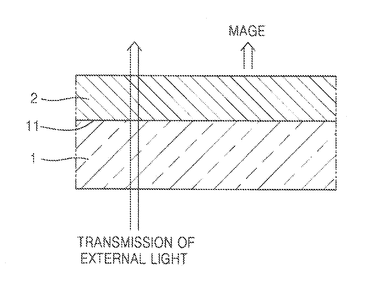
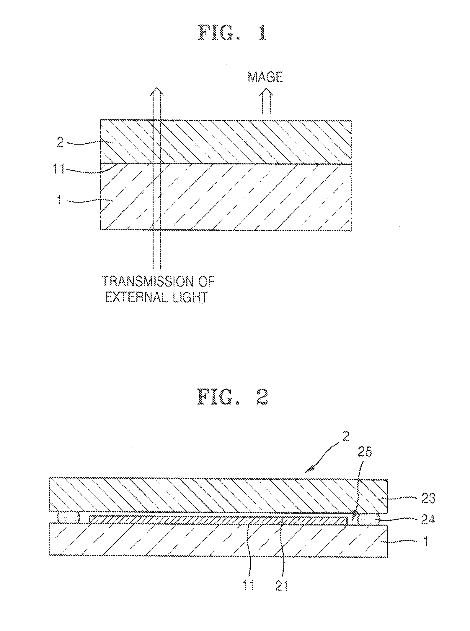
[0054]FIG. 1 is a cross-sectional view of an organic light-emitting display device according to an embodiment of the present invention.

[0055]Referring to FIG. 1, in the organic light-emitting display device, a display unit 2 is formed on a first surface 11 of a substrate 1.

[0056]When external light is incident on the organic light emitting display device, the external light sequentially penetrates the substrate 1 and the display unit 2.

[0057]As will be described later, the display unit 2 is formed to allow external light to penetrate therethrough. Referring to FIG. 1, the display unit 2 is formed in such a way that a user positioned at a side where an image is displayed can view an image below the substrate 1.

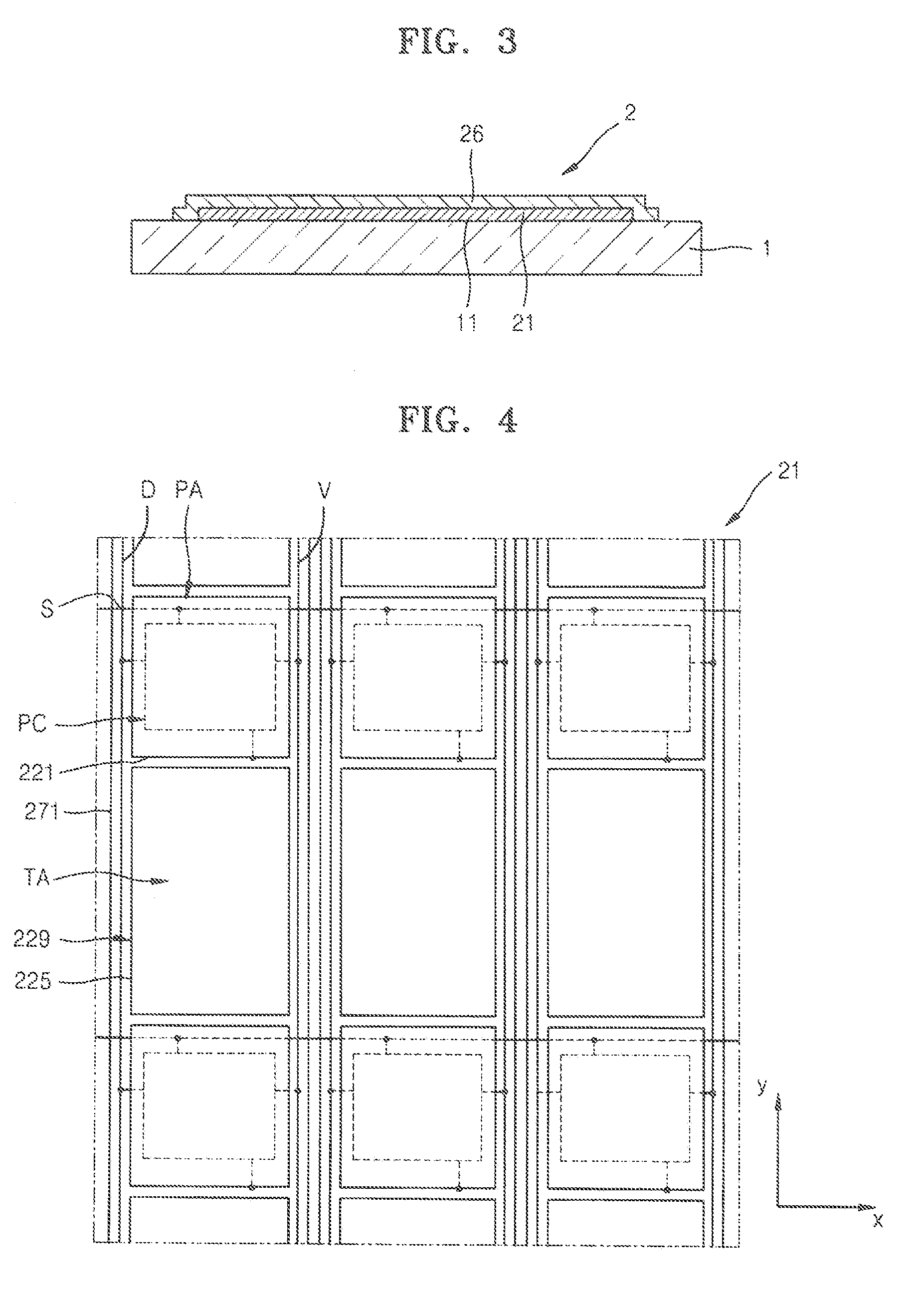
[0058]FIG. 2 is a cross-sectional view showing details of the organic light-emitting display device of FIG. 1 acco...


PUM


Abstract

An organic light-emitting display device, formed to be transparent, includes a substrate; a plurality of thin film transistors disposed on the substrate; a passivation layer covering the plurality of thin film transistors; a plurality of pixel electrodes disposed on the passivation layer and connected electrically to the plurality of thin film transistors, and overlapping and covering the plurality of thin film transistors; a first conductive unit disposed on the passivation layer to be disconnected electrically from the pixel electrodes; a pixel defining layer formed on the passivation layer to cover edges of the pixel electrodes; an opposite electrode facing the plurality of pixel electrodes, and covering at least part of the first conductive unit; an organic layer, including an emission layer, disposed between the pixel electrodes and the opposite electrode; and a second conductive unit connected electrically to a portion of the opposite electrode and the first conductive unit.

Description

CLAIM OF PRIORITY[0001]This application makes reference to, incorporates the same herein, and claims all benefits accruing under 35 U.S.C. §119 from an application earlier filed in the Korean Intellectual Property Office on the 5 of Mar. 2010 and there duly assigned Serial No. 10-2010-0020060.BACKGROUND OF THE INVENTION[0002]1. Field of the Invention[0003]The present invention relates to organic light-emitting display (OLED) devices and, more particularly, to a transparent organic light-emitting display device.[0004]2. Description of the Related Art[0005]Applications of organic light-emitting display devices range from personal portable devices such as MP3 players and mobile phones to television sets owing to having superior characteristics such as wide viewing angles, high contrast ratios, short response times, and low amounts of power consumption.[0006]An organic light-emitting display device has self-light emitting characteristics, and the weight and thickness of the organic ligh...

Claims


Application Information

Patent Timeline
Patent Type & Authority Applications(United States)
IPC IPC(8): H01L51/52
CPCH01L27/326H01L51/52H10K59/121H10K50/80H05B33/28H10K50/84H10K2102/351
Inventor CHUNG, JIN-KOO
Owner SAMSUNG DISPLAY CO LTD
Why Eureka
Try Eureka